Полупроводники. Каталог (2011 год) - часть 9


  Главная      Книги - Разные     Полупроводники. Каталог (2011 год)


поиск по сайту            правообладателям  


содержание      ..     7      8      9      10     ..


Полупроводники. Каталог (2011 год) - часть 9


SN75468, SN75469

DARLINGTON TRANSISTOR ARRAYS

SLRS023B – DECEMBER 1976 – REVISED SEPTEMBER 1995

3–5

POST OFFICE BOX 655303 

 DALLAS, TEXAS 75265

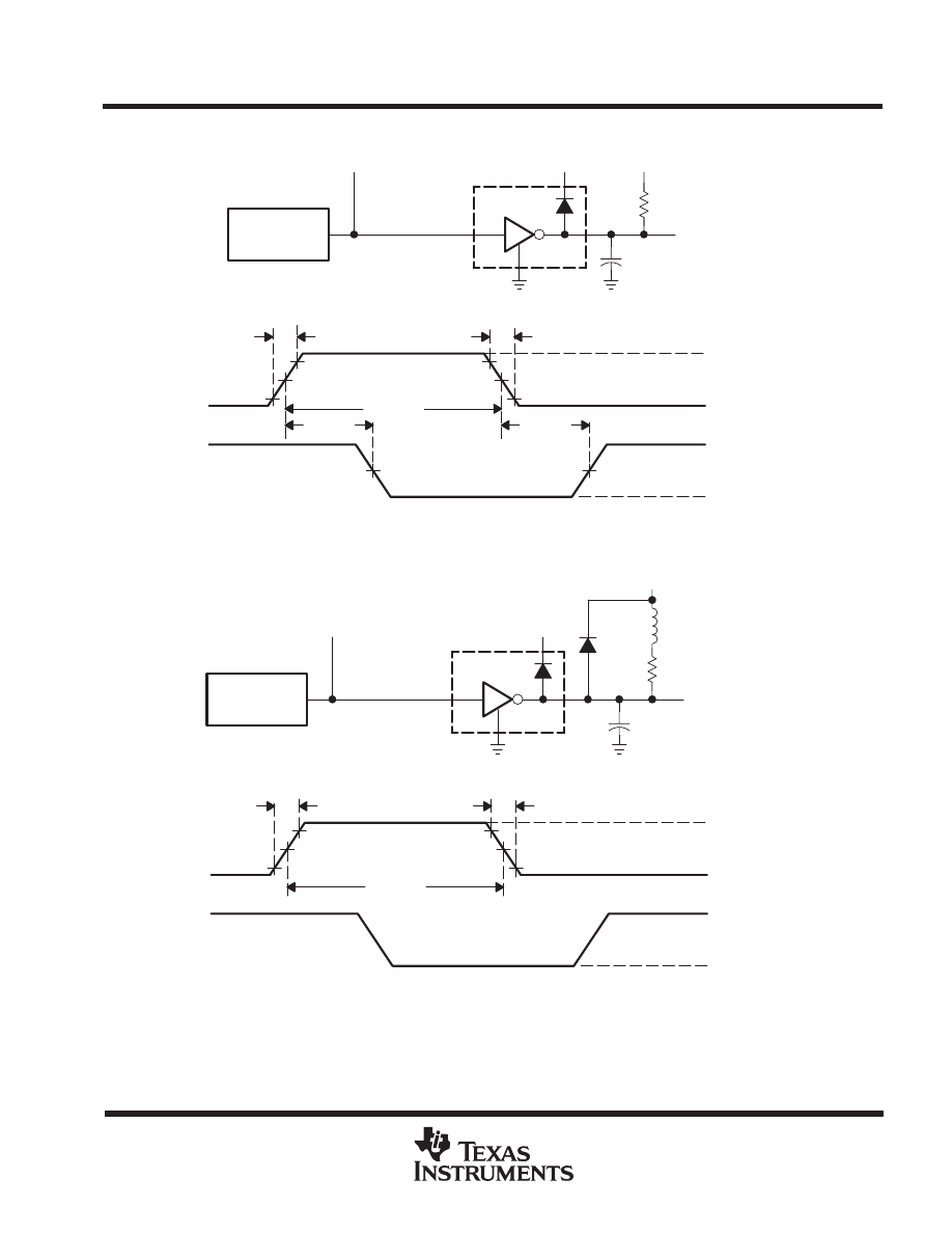
PARAMETER MEASUREMENT INFORMATION

Input

Open

VS = 50 V

RL = 163 

Output

CL = 15 pF
(see Note B)

90%

90%

50%

50%

10%

10%

50%

50%

tPHL

tPLH

0.5 

µ

s

 10 ns

 5 ns

VIH
(see Note C)

0 V

VOH

VOL

Input

Output

TEST CIRCUIT

VOLTAGE WAVEFORMS

Pulse

Generator

(see Note A)

Figure 9. Test Circuit and Voltage Waveforms

Input

Open

VS

200 

Output

CL = 15 pF
(see Note B)

90%

90%

1.5 V

1.5 V

10%

10%

40 

µ

s

 10 ns

 5 ns

VIH
(see Note C)

0 V

VOH

VOL

Input

Output

TEST CIRCUIT

VOLTAGE WAVEFORMS

1N3064

2 mH

Pulse

Generator

(see Note A)

Figure 10. Latch-Up Test Circuit and Voltage Waveforms

NOTES: A. The pulse generator has the following characteristics: PRR = 12.5 kHz, ZO = 50 

.

B. CL includes probe and jig capacitance.

C.  For testing the  ’468, VIH = 3 V; for the ’469, VIH = 8 V.

SN75468, SN75469
DARLINGTON TRANSISTOR ARRAYS

SLRS023B – DECEMBER 1976 – REVISED SEPTEMBER 1995

3–6

POST OFFICE BOX 655303 

 DALLAS, TEXAS 75265

TYPICAL CHARACTERISTICS

COLLECTOR-EMITTER

SATURATION VOLTAGE

vs

COLLECTOR CURRENT

(ONE DARLINGTON)

0

IC – Collector Current – mA

2.5

800

0

100

200

300

400

500

600

700

0.5

1

1.5

2

TA = 25

°

C

II = 250 mA
II = 350 mA

VCE(sat) – Collector-Emitter Saturation V

oltage – V

II = 350 mA

II = 250 mA

TA = 25

°

C

2

1.5

1

0.5

700

600

500

400

300

200

100

0

800

2.5

IC(tot) – Total Collector Current – mA

0

COLLECTOR-EMITTER

SATURATION VOLTAGE

vs

COLLECTOR CURRENT

(TWO DARLINGTONS PARALLELED)

Figure 11

Figure 12

V

CE(sat)

VCE(sat) – Collector-Emitter Saturation V

oltage – V

V

CE(sat)

II = 500 mA

II = 500 mA

2.25

1.75

1.25

0.75

0.25

2.25

1.75

1.25

0.75

0.25

Figure 13

COLLECTOR CURRENT

vs

INPUT CURRENT

0

II  – Input Current – mA

500

200

0

25

50

75

100

125

150

175

50

100

150

200

250

300

350

400

450

RL = 10 

TA = 25

°

C

VS = 8 V

IC – Collector Current – mA CI

VS = 10 V

SN75468, SN75469

DARLINGTON TRANSISTOR ARRAYS

SLRS023B – DECEMBER 1976 – REVISED SEPTEMBER 1995

3–7

POST OFFICE BOX 655303 

 DALLAS, TEXAS 75265

THERMAL INFORMATION

0

Duty Cycle – %

600

100

0

10

20

30

40

50

60

70

80

90

100

200

300

400

500

TA = 70

°

C

N = Number of Outputs

Conducting Simultaneously

N = 6
N = 7

N = 1

500

400

300

200

100

90

80

70

60

50

40

30

20

10

0

100

600

Duty Cycle – %

0

N = 7

TA = 70

°

C

D PACKAGE

MAXIMUM COLLECTOR CURRENT

vs

DUTY CYCLE

N  PACKAGE

MAXIMUM COLLECTOR CURRENT

vs

DUTY CYCLE

N = 5

N = 4

N = 3

N = 2

N = 1

N = 5

N = 4

N = 3

N = 2

IC – Maximum Collector Current – mA CI

N = 6

Conducting Simultaneously

N = Number of Outputs

IC – Maximum Collector Current – mA CI

Figure 14

Figure 15

SN75468, SN75469
DARLINGTON TRANSISTOR ARRAYS

SLRS023B – DECEMBER 1976 – REVISED SEPTEMBER 1995

3–8

POST OFFICE BOX 655303 

 DALLAS, TEXAS 75265

APPLICATION INFORMATION

SN75468

SN75468

SN75469

Lamp
Test

TTL
Output

CMOS
Output

VCC

+ V

VDD

+ V

VCC

+ V

RP

TTL
Output

1

2

3

4

5

6

9

10

11

12

13

14

15

16

8

7

1

2

3

4

5

6

9

10

11

12

13

14

15

16

8

7

1

2

3

4

5

6

9

10

11

12

13

14

15

16

8

7

Figure 16. TTL to Load

Figure 17. Buffer for Higher Current Loads

Figure 18. Use of Pullup Resistors to

Increase Drive Current

IMPORTANT NOTICE

Texas Instruments and its subsidiaries (TI) reserve the right to make changes to their products or to discontinue
any product or service without notice, and advise customers to obtain the latest version of relevant information
to verify, before placing orders, that information being relied on is current and complete. All products are sold
subject to the terms and conditions of sale supplied at the time of order acknowledgement, including those
pertaining to warranty, patent infringement, and limitation of liability.

TI warrants performance of its semiconductor products to the specifications applicable at the time of sale in
accordance with TI’s standard warranty. Testing and other quality control techniques are utilized to the extent
TI deems necessary to support this warranty. Specific testing of all parameters of each device is not necessarily
performed, except those mandated by government requirements.

CERTAIN APPLICATIONS USING SEMICONDUCTOR PRODUCTS MAY INVOLVE POTENTIAL RISKS OF
DEATH, PERSONAL INJURY, OR SEVERE PROPERTY OR ENVIRONMENTAL DAMAGE (“CRITICAL
APPLICATIONS”). TI SEMICONDUCTOR PRODUCTS ARE NOT DESIGNED, AUTHORIZED, OR
WARRANTED TO BE SUITABLE FOR USE IN LIFE-SUPPORT DEVICES OR SYSTEMS OR OTHER
CRITICAL APPLICATIONS. INCLUSION OF TI PRODUCTS IN SUCH APPLICATIONS IS UNDERSTOOD TO
BE FULLY AT THE CUSTOMER’S RISK.

In order to minimize risks associated with the customer’s applications, adequate design and operating
safeguards must be provided by the customer to minimize inherent or procedural hazards.

TI assumes no liability for applications assistance or customer product design. TI does not warrant or represent
that any license, either express or implied, is granted under any patent right, copyright, mask work right, or other
intellectual property right of TI covering or relating to any combination, machine, or process in which such
semiconductor products or services might be or are used. TI’s publication of information regarding any third
party’s products or services does not constitute TI’s approval, warranty or endorsement thereof.

 1998, Texas Instruments Incorporated

74VHC245

OCTAL BUS

TRANSCEIVER (3-STATE)

PRELIMINARY DATA

June 1999

ORDER CODES :

74VHC245M

74VHC245T

M

(Micro Package)

HIGH SPEED: t

PD

= 4.0 ns (TYP.) at V

CC

= 5V

LOW POWER DISSIPATION:
I

CC

= 4

µ

A (MAX.) at T

A

= 25

o

C

HIGH NOISE IMMUNITY:
V

NIH

= V

NIL

= 28% V

CC

(MIN.)

POWER DOWN PROTECTION ON CONTROL
INPUTS

SYMMETRICAL OUTPUT IMPEDANCE:
|I

OH

| = I

OL

= 8 mA (MIN)

BALANCED PROPAGATION DELAYS:
t

PLH

t

PHL

OPERATING VOLTAGE RANGE:
V

CC

(OPR) = 2V to 5.5V

PIN AND FUNCTION COMPATIBLE WITH
74 SERIES 245

IMPROVED LATCH-UP IMMUNITY

LOW NOISE V

OLP

= 0.9V (Max.)

DESCRIPTION
The 74VHC245 is an advanced high-speed
CMOS OCTAL BUS TRANSCEIVER (3-STATE)
fabricated with sub-micron silicon gate and
double-layer metal wiring C

2

MOS technology.

This IC is intended for two-way asynchronous
communication

between

data

busses;

the

direction of data trasmission is determined by the
level of the DIR input. The enable input G can be

T

(TSSOP Package)

used to disable the device so that the busses are
effectively isolated.
All inputs

and

outputs are

equipped with

protection circuits against static discharge, giving
them 2kV ESD immunity and transient excess
voltage.
IT IS PROHIBITED TO APPLY A SIGNAL TO A
TERMINAL WHEN IT IS IN OUTPUT MODE
AND WHEN A BUS TERMINAL IS FLOATING
(HIGH IMPEDANCE STATE) IT IS REQUESTED
TO FIX THE INPUT LEVEL BY MEANS OF
EXTERNAL

PULL

DOWN

OR

PULL

UP

RESISTOR.

PIN CONNECTION AND IEC LOGIC SYMBOLS


1/8

PIN DESCRIPTION

PIN No

SYMBOL

NAME AND FUNCT ION

1

DIR

Directional Control

2, 3, 4, 5,

6, 7, 8, 9

A1 to A8

Data Inputs/Outputs

18, 17, 16,
15, 14, 13,

12, 11

B1 to B8

Data Inputs/Outputs

19

G

Output Enable Input

10

GND

Ground (0V)

20

V

CC

Positive Supply Voltage

TRUTH TABLE

INPUT

F UNCTI ON

OUT PUT

G

DIR

A BUS

B BUS

L

L

OUTPUT

INPUT

A = B

L

H

INPUT

OUTPUT

B = A

H

X

Z

Z

Z

X:”H” or ”L”
Z: High impedance

INPUT EQUIVALENT CIRCUIT

ABSOLUTE MAXIMUM RATINGS

Symbol

Parameter

Val ue

Unit

V

CC

Supply Voltage

-0.5 to +7.0

V

V

I

DC Input Voltage (DIR, G)

-0.5 to +7.0

V

V

I/O

Bus I/O Voltage

-0.5 to V

CC

+ 0.5

V

V

O

DC Output Voltage

-0.5 to V

CC

+ 0.5

V

I

IK

DC Input Diode Current

- 20

mA

I

OK

DC Output Diode Current

±

20

mA

I

O

DC Output Current

±

25

mA

I

CC

or I

GND

DC V

CC

or Ground Current

±

75

mA

T

stg

Storage Temperature

-65 to +150

o

C

T

L

Lead Temperature (10 sec)

300

o

C

Absolute Maximum Ratings are those values beyond which damage to the device may occur. Functional operation under these condition is not implied.

RECOMMENDED OPERATING CONDITIONS

Symbol

Parameter

Valu e

Uni t

V

CC

Supply Voltage

2.0 to 5.5

V

V

I

Input Voltage (DIR, G)

0 to 5.5

V

V

I/O

Bus I/O Voltage

0 to V

CC

V

V

O

Output Voltage

0 to V

CC

V

T

op

Operating Temperature

-40 to +85

o

C

dt/dv

Input Rise and Fall Time (see note 1) (V

CC

= 3.3

±

0.3V)

(V

CC

= 5.0

±

0.5V)

0 to 100

0 to 20

ns/V
ns/V

1) V

IN

from 30% to70%of V

CC

74VHC245

2/8

DC SPECIFICATIONS

Symb ol

Parameter

T est Cond ition s

Val ue

Un it

V

CC

(V)

T

A

= 25

o

C

-40 to 85

o

C

Min.

Typ .

Max.

Min .

Max.

V

IH

High Level Input
Voltage

2.0

1.5

1.5

V

3.0 to 5.5

0.7V

CC

0.7V

CC

V

IL

Low Level Input
Voltage

2.0

0.5

0.5

V

3.0 to 5.5

0.3V

CC

0.3V

CC

V

OH

High Level Output
Voltage

2.0

I

O

=-50

µ

A

1.9

2.0

1.9

V

3.0

I

O

=-50

µ

A

2.9

3.0

2.9

4.5

I

O

=-50

µ

A

4.4

4.5

4.4

3.0

I

O

=-4 mA

2.58

2.48

4.5

I

O

=-8 mA

3.94

3.8

V

OL

Low Level Output
Voltage

2.0

I

O

=50

µ

A

0.0

0.1

0.1

V

3.0

I

O

=50

µ

A

0.0

0.1

0.1

4.5

I

O

=50

µ

A

0.0

0.1

0.1

3.0

I

O

=4 mA

0.36

0.44

4.5

I

O

=8 mA

0.36

0.44

I

OZ

High Impedance
Output Leakage
Current

5.5

V

I

= V

IH

or V

IL

V

O

= V

CC

or GND

±

0.25

±

2.5

µ

A

I

I

Input Leakage Current

0 to 5.5

V

I

= 5.5V or GND

±

0.1

±

1.0

µ

A

I

CC

Quiescent Supply
Current

5.5

V

I

= V

CC

or GND

4

40

µ

A

AC ELECTRICAL CHARACTERISTICS (Input t

r

= t

f

=3 ns)

Symb ol

Parameter

Test Co nditi on

Val ue

Un it

V

CC

(V)

C

L

(pF )

T

A

= 25

o

C

-40 to 85

o

C

Min.

Typ .

Max.

Min .

Max.

t

PLH

t

PHL

Propagation Delay
Time

3.3

(*)

15

5.8

8.4

1.0

10.0

ns

3.3

(*)

50

8.3

11.9

1.0

13.5

5.0

(**)

15

4.0

5.5

1.0

6.5

5.0

(**)

50

5.5

7.5

1.0

8.5

t

PLZ

t

PHZ

Output Disable Time

3.3

(*)

15

R

L

= 1K

8.5

13.2

1.0

15.5

ns

3.3

(*)

50

R

L

= 1K

11.0

16.7

1.0

19.0

5.0

(**)

15

R

L

= 1K

5.8

8.5

1.0

10.0

5.0

(**)

50

R

L

= 1K

7.3

10.6

1.0

12.0

t

PZL

t

PZH

Output Enable Time

3.3

(*)

50

R

L

= 1K

11.5

15.8

1.0

18.0

ns

5.0

(**)

50

R

L

= 1K

7.0

9.7

1.0

11.0

t

OSLH

t

OSHL

Output to Output Skew
Time (note 1)

3.3

(*)

50

1.5

1.5

ns

5.0

(**)

50

1.0

1.0

(*) Voltage range is 3.3V

±

0.3V

(**) Voltage range is 5V

±

0.5V

Note 1: Parameter guaranteed by design. t

soLH

= |t

pLHm

- t

pLHn

|, t

soHL

= |t

pHLm

- t

pHLn

|

74VHC245

3/8

CAPACITIVE CHARACTERISTICS

Symb ol

Parameter

Test Co nditi ons

Valu e

Un it

T

A

= 25

o

C

-40 to 85

o

C

Min.

T yp.

Max.

Mi n.

Max.

C

IN

Input Capacitance

4

10

10

pF

C

I/O

Bus Input Capacitance

8

pF

C

PD

Power Dissipation
Capacitance (note 1)

21

pF

1) C

PD

isdefined as the value of the IC’sinternal equivalent capacitance which is calculated fromthe operating current consumption without load. (Referto

Test Circuit).Average operting current can be obtained by the following equation. I

CC

(opr) = C

PD

V

CC

f

IN

+ I

CC

/8(per circuit)

TEST CIRCUIT

T EST

SW IT CH

t

PLH

, t

PHL

Open

t

PZL

, t

PLZ

V

CC

t

PZH

, t

PHZ

GND

C

L

= 15/50 pF or equivalent (includes jig and probe capacitance)

R

L

= R

1

= 1K

orequivalent

R

T

= Z

OUT

of pulse generator (typically 50

)

DYNAMIC SWITCHING CHARACTERISTICS

Symb ol

Parameter

T est Cond ition s

Val ue

Un it

V

CC

(V)

T

A

= 25

o

C

-40 to 85

o

C

Min.

Typ .

Max.

Min .

Max.

V

OLP

Dynamic Low Voltage
Quiet Output (note 1, 2)

5.0

C

L

= 50 pF

0.6

0.9

V

V

OLV

-0.9

-0.6

V

IHD

Dynamic High Voltage
Input (note 1, 3)

5.0

3.5

V

IL D

Dynamic Low Voltage
Input (note 1, 3)

5.0

1.5

1) Worst case package.
2) Max number of outputs defined as (n). Data inputs are driven 0V to 5.0V, (n -1) outputs switching and one output at GND.
3) Max number of data inputs (n) switching. (n-1) switching 0V to5.0V. Inputs under test switching: 5.0V to threshold (V

ILD

), 0V to threshold (V

IHD

), f=1MHz.

74VHC245

4/8

WAVEFORM 1: PROPAGATION DELAYS (f=1MHz; 50% duty cycle)

WAVEFORM 2: OUTPUT ENABLE AND DISABLE TIME (f=1MHz; 50% duty cycle)

74VHC245

5/8

DIM.

mm

inch

MIN.

TYP.

MAX.

MIN.

TYP.

MAX.

A

2.65

0.104

a1

0.10

0.20

0.004

0.007

a2

2.45

0.096

b

0.35

0.49

0.013

0.019

b1

0.23

0.32

0.009

0.012

C

0.50

0.020

c1

45 (typ.)

D

12.60

13.00

0.496

0.512

E

10.00

10.65

0.393

0.419

e

1.27

0.050

e3

11.43

0.450

F

7.40

7.60

0.291

0.299

L

0.50

1.27

0.19

0.050

M

0.75

0.029

S

8 (max.)

P013L

SO-20 MECHANICAL DATA

74VHC245

6/8

DIM.

mm

inch

MIN.

TYP.

MAX.

MIN.

TYP.

MAX.

A

1.1

0.433

A1

0.05

0.10

0.15

0.002

0.004

0.006

A2

0.85

0.9

0.95

0.335

0.354

0.374

b

0.19

0.30

0.0075

0.0118

c

0.09

0.2

0.0035

0.0079

D

6.4

6.5

6.6

0.252

0.256

0.260

E

6.25

6.4

6.5

0.246

0.252

0.256

E1

4.3

4.4

4.48

0.169

0.173

0.176

e

0.65 BSC

0.0256 BSC

K

0

o

4

o

8

o

0

o

4

o

8

o

L

0.50

0.60

0.70

0.020

0.024

0.028

c

E

b

A2

A

E1

D

1

PIN 1 IDENTIFICATION

A1

L

K

e

TSSOP20 MECHANICAL DATA

74VHC245

7/8

Information furnished is believed to be accurate and reliable. However, STMicroelectronics assumes no responsibility for the consequences
of use of such information nor for any infringement of patents or other rights of third parties which may result from its use. No license is
granted by implication or otherwise under any patent or patent rights of STMicroelectronics. Specification mentioned in this publication are
subject to change without notice. This publication supersedes and replaces all information previously supplied. STMicroelectronics products
are not authorized for use as critical components in life support devices or systems without express written approval of STMicroelectronics.

The ST logo is a trademark of STMicroelectronics

1999 STMicroelectronics – Printed in Italy – All Rights Reserved

STMicroelectronics GROUP OF COMPANIES

Australia - Brazil - Canada - China - France - Germany - Italy - Japan - Korea - Malaysia - Malta - Mexico - Morocco - The Netherlands -

Singapore - Spain - Sweden - Switzerland - Taiwan - Thailand - United Kingdom - U.S.A.

http://www.st.com

.

74VHC245

8/8

 Semiconductor Components Industries, LLC, 2013

May, 2013 

 Rev. 9

1

Publication Order Number:

MC14514B/D

MC14514B, MC14515B

4-Bit Transparent Latch /
4-to-16 Line Decoder

The MC14514B and MC14515B are two output options of a 4 to 16

line decoder with latched inputs. The MC14514B (output active high
option) presents a logical “1” at the selected output, whereas the
MC14515B (output active low option) presents a logical “0” at the
selected output. The latches are R

S type flip

flops which hold the

last input data presented prior to the strobe transition from “1” to “0”.
These high and low options of a 4

bit latch / 4 to 16 line decoder are

constructed with N

channel and P

channel enhancement mode

devices in a single monolithic structure. The latches are R

S type

flip

flops and data is admitted upon a signal incident at the strobe

input, decoded, and presented at the output.

These complementary circuits find primary use in decoding

applications where low power dissipation and/or high noise immunity
is desired.

Features

Supply Voltage Range = 3.0 Vdc to 18 Vdc

Capable of Driving Two Low

power TTL Loads or One Low

power

Schottky TTL Load  the Rated Temperature Range

These Devices are Pb

Free and are RoHS Compliant

NLV Prefix for Automotive and Other Applications Requiring

Unique Site and Control Change Requirements; AEC

Q100

Qualified and PPAP Capable

MAXIMUM RATINGS 

(Voltages Referenced to V

SS

)

Parameter

Symbol

Value

Unit

DC Supply Voltage Range

V

DD

0.5 to +18.0

V

Input or Output Voltage Range

(DC or Transient)

V

in

, V

out

0.5 to V

DD

+0.5

V

Input or Output Current (DC or Transient)

per Pin

I

in

, I

out

±

10

mA

Power Dissipation per Package (Note 1)

P

D

500

mW

Ambient Temperature Range

T

A

55 to +125

°

C

Storage Temperature Range

T

stg

65 to +150

°

C

Lead Temperature (8

Second Soldering)

T

L

260

°

C

Stresses exceeding Maximum Ratings may damage the device. Maximum

Ratings are stress ratings only. Functional operation above the Recommended

Operating Conditions is not implied. Extended exposure to stresses above the

Recommended Operating Conditions may affect device reliability.

1. Temperature Derating: Plastic “P and D/DW”

Packages: – 7.0 mW/

_

C From 65

_

C To 125

_

C

This device contains protection circuitry to guard against damage due to high

static voltages or electric fields. However, precautions must be taken to avoid
applications of any voltage higher than maximum rated voltages to this
high

impedance circuit. For proper operation, V

in

 and V

out

 should be constrained

to the range V

SS


v

 (V

in

 or V

out

v

 V

DD

.

Unused inputs must always be tied to an appropriate logic voltage level

(e.g., either V

SS

 or V

DD

). Unused outputs must be left open.

xx

=  14 or 15

A

=  Assembly Location

WL

=  Wafer Lot

YY

=  Year

WW = Work Week
G

=  Pb

Free Package

MARKING DIAGRAM

1

24

SOIC

24

DW SUFFIX

CASE 751E

145xxB

AWLYYWWG

See detailed ordering and shipping information in the package
dimensions section on page 2 of this data sheet.

ORDERING INFORMATION

http://onsemi.com

S5

S7

D2

D1

ST

S3

S4

S6

S10

D3

D4

INH

V

DD

S15

S14

S9

5

4

3

2

1

10

9

8

7

6

14

15

16

17

18

19

20

13

11

12

21

22

23

24

S13

S12

S8

S11

S0

V

SS

S2

S1

PIN ASSIGNMENT

MC14514B, MC14515B

http://onsemi.com

2

Data Inputs

Selected Output

MC14514 = Logic “1”

Inhibit

D

C

B

A

MC14515 = Logic “0”

0

0

0

0

0

S0

0

0

0

0

1

S1

0

0

0

1

0

S2

0

0

0

1

1

S3

0

0

1

0

0

S4

0

0

1

0

1

S5

0

0

1

1

0

S6

0

0

1

1

1

S7

0

1

0

0

0

S8

0

1

0

0

1

S9

0

1

0

1

0

S10

0

1

0

1

1

S11

0

1

1

0

0

S12

0

1

1

0

1

S13

0

1

1

1

0

S14

0

1

1

1

1

S15

1

X

X

X

X

All Outputs = 0, MC14514
All Outputs = 1, MC14515

DECODE TRUTH TABLE


(Strobe = 1)*

X = Don’t Care

*Strobe = 0, Data is latched

BLOCK DIAGRAM

V

DD 

= PIN 24

V

SS

 = PIN 12

4 TO 16

DECODER

TRANSPARENT

LATCH

STROBE

INHIBIT

2

3

1

21

22

23

DATA 1

DATA 2

DATA 3

DATA 4

A

B

C

D

20

17

18

4

5

6

7

8

10

9

11

19

16

13

14

15

A B C D

A B C D
A B C D

A B C D
A B C D

A B C D

A B C D
A B C D

A B C D
A B C D

A B C D

A B C D
A B C D

A B C D
A B C D

A B C D

S15

S14

S13

S12

S11

S10

S9

S8

S7

S6

S5

S4

S3

S2

S1

S0

ORDERING INFORMATION

Device

Package

Shipping

MC14514BDWR2G

SOIC

24

(Pb

Free)

1000 / Tape & Reel

NLV14514BDWR2G*

MC14515BDWR2G

SOIC

24

(Pb

Free)

1000 / Tape & Reel

NLV14515BDWR2G*

†For information on tape and reel specifications, including part orientation and tape sizes, please refer to our Tape and Reel Packaging

Specifications Brochure, BRD8011/D.

*NLV Prefix for Automotive and Other Applications Requiring Unique Site and Control Change Requirements; AEC

Q100 Qualified and PPAP

Capable.

MC14514B, MC14515B

http://onsemi.com

3

ÎÎÎÎÎÎÎÎÎÎÎÎÎÎÎÎÎÎÎÎÎÎÎÎÎÎÎÎÎÎÎÎÎ

ÎÎÎÎÎÎÎÎÎÎÎÎÎÎÎÎÎÎÎÎÎÎÎÎÎÎÎÎÎÎÎÎÎ

ELECTRICAL CHARACTERISTICS 

(Voltages Referenced to V

SS

)

Characteristic

Symbol

V

DD

Vdc

 55

_

C

25

_

C

125

_

C

Unit

Min

Max

Min

Typ

(Note 2)

Max

Min

Max

Output Voltage

“0” Level

V

in

 =  V

DD

 or 0 

“1” Level

V

in

 = 0 or V

DD

V

OL

5.0

10

15

0.05

0.05

0.05

0

0

0

0.05

0.05

0.05

0.05

0.05

0.05

Vdc

V

OH

5.0

10

15

4.95

9.95

14.95

4.95

9.95

14.95

5.0

10

15

4.95

9.95

14.95

Vdc

Input Voltage

“0” Level

(V

O

 = 4.5 or 0.5 Vdc) 

(V

O

 = 9.0 or 1.0 Vdc) 

(V

O

 = 13.5 or 1.5 Vdc)

“1” Level

(V

O

 = 0.5 or 4.5 Vdc) 

(V

O

 = 1.0 or 9.0 Vdc) 

(V

O

 = 1.5 or 13.5 Vdc)

V

IL

5.0

10

15

1.5

3.0

4.0

2.25

4.50

6.75

1.5

3.0

4.0

1.5

3.0

4.0

Vdc

V

IH

5.0

10

15

3.5

7.0

11

3.5

7.0

11

2.75

5.50

8.25

3.5

7.0

11

Vdc

Output Drive Current

(V

OH

 = 2.5 Vdc) 

Source

(V

OH

 = 4.6 Vdc)

(V

OH

 = 9.5 Vdc)

(V

OH

 = 13.5 Vdc)

(V

OL

 = 0.4 Vdc) 

Sink

(V

OL

 = 0.5 Vdc)

(V

OL

 = 1.5 Vdc)

I

OH

5.0

5.0

10

15

– 1.2

– 0.25

– 0.62

– 1.8

– 1.0

– 0.2

– 0.5

– 1.5

– 1.7

– 0.36

– 0.9

– 3.5

– 0.7

– 0.14

– 0.35

– 1.1

mAdc

I

OL

5.0

10

15

0.64

1.6

4.2

0.51

1.3

3.4

0.88

2.25

8.8

0.36

0.9

2.4

mAdc

Input Current

I

in

15

±

0.1

±

0.00001

±

0.1

±

1.0

m

Adc

Input Capacitance (V

in

 = 0)

C

in

5.0

7.5

pF

Quiescent Current (Per Package)

I

DD

5.0

10

15

5.0

10

20

0.005

0.010

0.015

5.0

10

20

150

300

600

m

Adc

Total Supply Current (Note 3, 4)

(Dynamic plus Quiescent,

Per Package) 

(C

L

 = 50 pF on all outputs, all

buffers switching)

I

TL

5.0

10

15

I

T

 = (1.35 

m

A/kHz) f + I

DD

I

T

 = (2.70 

m

A/kHz) f + I

DD

I

T

 = (4.05 

m

A/kHz) f + I

DD

m

Adc

2. Data labelled “Typ” is not to be used for design purposes but is intended as an indication of the IC’s potential performance.

3. The formulas given are for the typical characteristics only at 25

_

C.

4. To calculate total supply current at loads other than 50 pF: I

T

(C

L

) = I

T

(50 pF) + (C

L

 – 50) Vfk where: I

T

 is in 

m

A (per package), C

L

 in pF, 

V = (V

DD

 – V

SS

) in volts, f in kHz is input frequency, and k = 0.002.


содержание      ..     7      8      9      10     ..