Полупроводники. Каталог (2011 год) - часть 6


  Главная      Книги - Разные     Полупроводники. Каталог (2011 год)


поиск по сайту            правообладателям  


содержание      ..     4      5      6      7     ..


Полупроводники. Каталог (2011 год) - часть 6


12/26

¡ Semiconductor

MSM82C51A-2RS/GS/JS

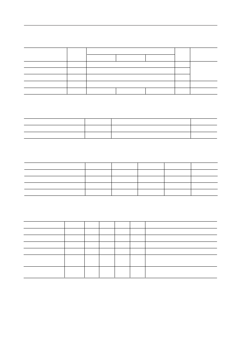
ABSOLUTE MAXIMUM RATING

–55 to +150

MSM82C51A-2RS

Power Supply Voltage

V

CC

–0.5 to +7

V

Input Voltage

V

IN

–0.5 to V

CC  

+0.5

V

Output Voltage

V

OUT

–0.5 to V

CC  

+0.5

V

Storage Temperature

T

STG

°C

Power Dissipation

P

D

0.7

W

Parameter

Unit

Symbol

With respect

to GND

Ta = 25°C

Conditions

Rating

MSM82C51A-2GS MSM82C51A-2JS

0.9

0.9

OPERATING RANGE

Range

Power Supply Voltage

V

CC

3 - 6

V

Operating Temperature

T

op

–40 to 85

°C

Parameter

Unit

Symbol

RECOMMENDED OPERATING CONDITIONS

DC CHARACTERISTICS

Typ.

Max.

"L" Output Voltage

V

OL

0.45

V

"H" Output Voltage

V

OH

V

Parameter

Unit

Symbol

Min.

3.7

I

OL 

= 2.5 mA

I

OH 

= –2.5 mA

Measurement Conditions

Input Leak Current

I

LI

10

m

A

Output Leak Current

I

LO

10

m

A

–10
–10

£ 

V

IN 

£ 

V

CC

£ 

V

OUT 

£ 

V

CC

Operating Supply
Current

5

mA

Asynchronous X64 during Transmitting/
Receiving

Standby Supply
Current

100

m

A

I

CCO

I

CCS

All Input voltage shall be fixed at V

CC 

or 

GND level.

(V

CC

 = 4.5 to 5.5 V  Ta = –40°C to +85°C)

Typ.

Power Supply Voltage

V

CC

5

V

T

op

+25

"L" Input Voltage

V

IL

"H" Input Voltage

V

IH

Min.

4.5

–40

–0.3

2.2

Max.

5.5

+85

+0.8

V

CC 

+0.3

Parameter

Unit

Symbol

°C

V
V

Operating Temperature

13/26

¡ Semiconductor

MSM82C51A-2RS/GS/JS

AC  CHARACTERISTICS

CPU Bus Interface Part

Max.

Address Stable before 

RD

t

AR

ns

Parameter

Unit

Symbol

Min.

20

Note 2

Remarks

Address Hold Time for 

RD

t

RA

ns

RD

 Pulse Width

t

RR

ns

20

130

Note 2

Data Delay from 

RD

t

RD

100

ns

RD

 to Data Float

t

DF

75

ns

10

Recovery Time between 

RD

t

RVR

t

CY

Address Stable before 

WR

t

AW

ns

6

20

Note 5
Note 2

Address Hold Time for 

WR

t

WA

ns

20

Note 2

WR

 Pulse Width

t

WW

ns

100

Data Set-up Time for 

WR

t

DW

ns

Data Hold Time for 

WR

t

WD

ns

100

0


Recovery Time between 

WR

t

RVW

t

CY

6

Note 4

RESET Pulse Width

t

RESW

t

CY

6

(V

CC

 = 4.5 to 5.5 V,  Ta = –40 to 85°C)

14/26

¡ Semiconductor

MSM82C51A-2RS/GS/JS

Serial Interface Part

Notes: 1. AC characteristics are measured at 150 pF capacity load as an output load based on 0.8 V at

low level and 2.2 V at high level for output and 1.5 V for input.

2. Addresses are 

CS

 and C/

D

.

3. f

TX

 or f

RX


£ 

1/(30 Tcy) 1

¥

 Baud

f

TX

 or f

RX


£ 

1/(5 Tcy)

16

¥

, 64

¥

 Baud

4. This recovery time is mode Initialization only.  Recovery time between command writes for

Asynchronous Mode is 8 t

CY

 and for Synchronous Mode is 18 t

CY

.

Write Data is allowed only when TXRDY = 1.

5. This recovery time is Status read only.

Read Data is allowed only when RXRDY = 1.

6. Status update can have a maximum delay of 28 clock periods from event affecting the status.

Max.

Main Clock Period

t

CY

ns

Parameter

Unit

Symbol

Min.

160

Note 3

Remarks

Clock Low Tme

t

f

ns

Clock High Time

t

f

t

CY

 –50

ns

50
70


Clock Rise/Fall Time

t

r, 

t

f

20

ns

TXD Delay from Falling Edge of 

TXC

t

DTX

1

m

S

Transmitter Clock Frequency    

f

TX

64

kHz

f

TX

615

kHz

DC
DC

Note 3

f

TX

615

kHz

DC

¥

 Baud

16 

¥

 Baud

64 

¥

 Baud

Transmitter Clock Low Time 

t

TPW

t

CY

¥

 Baud

t

TPW

t

CY

Transmitter Clock High Time 

t

TPD

13

2

15

t

CY

16 

¥

, 64 

¥

 Baud

¥

 Baud


t

TPD

t

CY

3

16 

¥

, 64 

¥

 Baud

Receiver Clock Frequency 

f

RX

64

DC

kHz

¥

 Baud

f

RX

615

kHz

f

RX

615

kHz

DC
DC

16 

¥

 Baud

64 

¥

 Baud

Note 3

Receiver Clock Low Time 

t

RPW

t

CY

13

t

RPW

t

CY

2

¥

 Baud

16 

¥

, 64 

¥

 Baud

Receiver Clock High Time  

t

RPD

t

CY

t

RPD

t

CY

15

3

¥

 Baud

16 

¥

, 64 

¥

 Baud


Time from the Center of Last Bit to the Rise of 

TXRDY

t

TXRDY

8

t

CY

Time from the Leading Edge of 

WR

 to the Fall 

of TXRDY

t

TXRDY CLEAR

400

ns

Time From the Center of Last Bit to the Rise of RXRDY

t

RXRDY

26

t

CY

Time from the Leading Edge of 

RD

 to the Fall

of RXRDY

t

RXRDY CLEAR

400

ns

Internal SYNDET Delay Time from Rising Edge of 

RXC

t

IS

26

t

CY

MODEM Control Signal Delay Time from Rising Edge 

of 

WR

t

WC

t

CY

8

MODEM Control Signal Setup Time for Falling Edge 

of 

RD

t

CR

t

CY

20

RXD Setup Time for Rising Edge of 

RXC

 (1X Baud)

t

RXDS

t

CY

11

RXD Hold Time for Falling Edge of 

RXC

 (1X Baud)

t

RXDH

t

CY

17

SYNDET Setup Time for 

RXC

t

ES

t

CY

18

TXE Delay Time from the Center of Last Bit

t

TXEMPTY

t

CY

20

(V

CC

 = 4.5 to 5.5 V,  Ta = –40 to 85°C)

15/26

¡ Semiconductor

MSM82C51A-2RS/GS/JS

TIMING  CHART

Sytem Clock Input

t

f

t

r

t

f

t

f

t

CY

CLK

Receiver Clock and Data

Transmitter Clock and Data

t

TPW

TXC

 (1 

¥

 MODE)

t

TPD

t

DTX

t

DTX

TXC

 (16 

¥

 MODE)

TXD

RXC

 (1 

¥

 Mode)

t

RPW

RXC

 (16 

¥

 Mode)

RXD

INT Sampling

Pulse

(RXBAUD Counter starts here)

Start bit

8RXC Periods

(16

¥

Mode)

16 RXC Periods (16


¥


Mode)

Data bit

Data bit

t

RPD

3t

CY

3t

CY

t

f

16/26

¡ Semiconductor

MSM82C51A-2RS/GS/JS

Read Control or Input Port Cycle (CPU 

¨

 USART)

Write Control or Output Port Cycle (CPU 

Æ

 USART)

Read Data Cycle (CPU 

¨

 USART)

t

RR

t

RD

t

DF

Data Out Active

t

AR

t

RA

t

AR

t

RA

t

RXRDY Clear

Data Float

Data Float

RD

DATA OUT (D. B.)

RXRDY

CS

C/

D

Write Data Cycle (CPU 

Æ

 USART)

t

TXRDY Clear

t

DW

t

WD

t

AW

t

WA

t

AW

t

WA

Data Stable

Don't Care

Don't Care

WR

DATA IN (D. B.)

TXRDY

CS

C/

D

t

WW

t

CR

t

RR

t

RD

t

AR

t

RA

t

AR

t

RA

t

DF

Data Float

Data Out Active

Data Float

DSR

CTS

DATA OUT

(D. B.)

RD

C/

D

CS

DTR

RTS

DATA IN

(D. B.)

WR

C/

D

CS

t

WW

t

WC

t

AW

t

WA

t

AW

t

WA

Data Stable

Don't Care

Don't Care

t

WD

t

DW

17/26

¡ Semiconductor

MSM82C51A-2RS/GS/JS

Transmitter Control and Flag Timing (ASYNC Mode)

DATA CHAR 1

DATA CHAR 2

DATA CHAR 3

DATA CHAR 4

START BIT

STOP BIT

Wr TxEn

Wr SBRK

t

TXEMPTY

t

TXRDY

CTS

TXEMPTY

TXRDY

(STATUS BIT)

TXRDY

(PIN)

C/

D

WR

TXD

0 1 2 3 4 5 6

Wr DATA 1

Wr DATA 2

Wr DATA 3

Wr DATA 4

Note: 

The wave-form chart is based on the case of 7-bit data length + parity bit + 2 stop bit.

Transmitter Control and Flag Timing (SYNC Mode)

Receiver Control and Flag Timing (ASYNC Mode)

Data CHAR 1 Data CHAR 2 Data CHAR 3

Break

Data Bit Start Bit Stop Bit Parity Bit

RxEn Err Res

RxEn

t

RXRDY

DATA

CHAR2

Lost

Wr RxEn

BREAK DETECT

FRAMING ERROR

(Status Bit)

OVERRUN ERROR

(Status Bit)

RXRDY

C/

D

WR

RD

RXDATA

Wr Error

Rd Data

Note:

 The wave-form chart is based on the case of 7 data bit length + parity bit + 2 stop bit.

0 1 2 3 4

0 1 2 3 4

0 1 2 3 4

0 1 2 3 4  0 1 2 3 4

0 1 2 3 4

0 1 2 3 4

0 1 2 3 4

0 1

Data

CHAR1

Data

CHAR2

SYNC

CHAR1 SYNC CHAR2

SYNC

CHAR3

Data

CHAR4

Marking

State

Spacing

State

Marking

State

Data

CHAR5

SYNC

CHAR     ETC

PAR

PAR

PAR

PAR

PAR

PAR

PAR

PAR

Wr Commond

SBRK

Wr Data

CHAR5

CTS

TXEMPTY

TXRDY

(StatusBit)

TXRDY (Pin)

C/

D

WR

TXD

Wr Data

CHAR1

Marking State

Wr Data

CHAR2

Wr Data

CHAR3

Wr Data

CHAR4

Note:

 The wave-form chart is based on the case of 5 data bit length + parity bit and 2 synchronous charactors.

18/26

¡ Semiconductor

MSM82C51A-2RS/GS/JS

Receiver Control and Flag Timing (SYNC Mode)

x x x x x x 0 1 2 3 4

0 1 2 3 4

0 1 2 3 4

0 1 2 3 4

0 1 2 3 4

0 1 2 3 4

0 1 2 3 4

x x x x x x x

0 1 2 3 4

0 1 x 3 4

SYNDET

(Pin) (Note 1)

SYNDET (SB)

OVERRUN

ERROR (SB)

RXRDY (PIN)

C/

D

WR

RD

RXD

RXC

Don't

Care

SYNC

CHAR 1

SYNC

CHAR 2

Data

CHAR 1

Data

CHAR 2

Data

CHAR 3

SYNC

CHAR 1

SYNC

CHAR 2 Don't Care

Data

CHAR 1

Data

CHAR 2

ETC

CHAR ASSY Begins

Exit Hunt Mode

Set SYNDET

Exit Hunt Mode

Set SYNDET (Status bit)

Set SYNDET (Status bit)

CHAR ASSY

Begins

Wr EH

RxEn

Rd Data

CHAR 1

Rd Status

Wr Err Res

Rd Data

CHAR 3

Rd SYNC

CHAR 1

Rd Status

Wr EHo

Rd Status

Data 

CHAR2

Lost

t

IS

t

ES

(Note 2)

Note:

PAR

PAR

PAR

PAR

PAR

PAR

PAR

PAR

PAR

PAR

1. Internal Synchronization is based on the case of 5 data bit length + parity bit and 2 synchronous charactor.
2. External Synchronization is based on the case of 5 data bit length + parity bit.

Note: 1. Half-bit processing for the start bit

When the MSM82C51A-2 is used in the asynchronous mode, some problems are

caused in the processing for the start bit whose length is smaller than the 1-data bit

length. (See Fig. 1.)

2. Parity flag after a break signal is received (See Fig. 2.)

When the MSM82C51A-2 is used in the asynchrous mode, a parity flag may be set

when the next normal data is read after a break signal is received.
A parity flag is set when the rising edge of the break signal (end of the break signal)

is changed between the final data bit and the parity bit, through a RXRDY signal may

not be outputted.
If this occurs, the parity flag is left set when the next normal dats is received, and the

received data seems to be a parity error.

Smaller than 7-Receiver Clock Length

¥

16

Start bit Length

Mode

Operation

The short start bit is ignored. (Normal)

Smaller than 31-Receiver Clock Length

¥

64

8-Receiver Clock Length

¥

16

The short start bit is ignored. (Normal)
Data cannot be received correctly due to a malfunction.

32-Receiver Clock Length

¥

64

Data cannot be received correctly due to a malfunction.

9 to 16-Receiver Clock Length

¥

16

The bit is regarded as a start bit. (normal)

33 to 64-Receiver Clock Length

¥

64

The bit is regarded as a start bit. (normal)

19/26

¡ Semiconductor

MSM82C51A-2RS/GS/JS

Half-bit Processing Timing Chart for the Start bit (Fig. 1)

ST D

0

D

1

D

2

D

3

D

4

D

5

D

6

D

7

P SP

ST D

0

D

1

D

2

D

3

D

4

D

5

D

6

D

7

P SP

RXD

RXRDY

ST

ST D

0

D

1

D

2

D

3

D

4

D

5

D

6

D

7

P SP

RXD

RXRDY

A RXRDY signal is outputted during data
reception due to a malfunction.

ST

ST D

0

D

1

D

2

D

3

D

4

D

5

D

6

D

7

P SP

RXD

RXRDY

ST:
SP:
P:
D

0

 - D

7

:

Start bit
Stop bit
Parity bit
Data bits

ST

ST D

0

D

1

D

2

D

3

D

4

D

5

D

6

D

7

P SP

RXD

RXRDY

Normal Operation

The Start bit Is Shorter Than a 1/2 Data bit

The Start bit Is a 1/2 Data bit (A problem of MSM82C51A-2)

The Start bit Is Longer Than a 1/2 Data bit

20/26

¡ Semiconductor

MSM82C51A-2RS/GS/JS

Break Signal Reception Timing and Parity Flag (Fig. 2)

ST D

0

D

7

P SP ST D

0

D

7

P SP ST D

0

D

1

D

2

D

3

D

4

D

5

D

6

D

7

P

BIT POS.

RXD

RXRDY

A parity flag is set, but, no RXRDYsignal
is outputted.

SP

ST D

0

D

7

P SP ST D

0

D

7

P SP ST D

0

D

1

D

2

D

3

D

4

D

5

D

6

D

7

P

BIT POS.

RXD

RXRDY

No parity flag is set. and no RXRDY signal
is outputted.

ST D

0

D

7

P SP ST D

0

D

7

P SP ST D

0

D

1

D

2

D

3

D

4

D

5

D

6

D

7

P

BIT POS.

RXD

RXRDY

A parity flag is set. and a RXRDY signal
is outputted.

SP

Normal Operation

Bug Timing

Normal Operation

SP

21/26

¡ Semiconductor

MSM82C51A-2RS/GS/JS

NOTICE ON REPLACING LOW-SPEED DEVICES WITH HIGH-SPEED DEVICES

The  conventional low speed devices are replaced by high-speed devices as shown below.
When you want to replace your low speed devices with high-speed devices, read the replacement
notice given on the next pages.

High-speed device (New)

Low-speed device (Old)

Remarks

M80C85AH

M80C85A/M80C85A-2

8bit MPU

M80C86A-10

M80C86A/M80C86A-2

16bit MPU

M80C88A-10

M80C88A/M80C88A-2

8bit MPU

M82C84A-2

M82C84A/M82C84A-5

Clock generator

M81C55-5

M81C55

RAM.I/O, timer

M82C37B-5

M82C37A/M82C37A-5

DMA controller

M82C51A-2

M82C51A

USART

M82C53-2

M82C53-5

Timer

M82C55A-2

M82C55A-5

PPI

22/26

¡ Semiconductor

MSM82C51A-2RS/GS/JS

Differences between MSM82C51A and MSM82C51A-2

1) Manufacturing Process

These devices use a 3 

m

 Si-Gate CMOS process technology and have the same chip size.

2) Function

These devices have the same logics except for changes in AC characteristics listed in (3-2).

3) Electrical Characteristics
3-1) DC  Characteristics

Although the output voltage characteristics of these devices are identical, but the measurement

conditions of the MSM82C51A-2 are more restricted than the MSM82C51A.

3-2) AC  Characteristics

As shown above, the MSM82C51A-2 satisfies the characteristics of the MSM82C51A.

Parameter

Symbol

MSM82C51A

MSM82C51A-2

RD

 Pulse Width

250 ns minimum

130 ns minimum

t

RR

RD

 Rising to Data Difinition

200 ns maximum

100 ns maximum

t

RD

RD

 Rising to Data Float

100 ns maximum

75 ns minimum

t

RF

WR

 Pulse Width

250 ns minimum

100 ns minimum

t

WW

Data Setup Time for 

WR

 Rising

150 ns minimum

100 ns minimum

t

DW

Data Hold Time for 

WR

 Rising

20 ns minimum

0 ns minimum

t

WD

Master Clock Period

250 ns minimum

160 ns minimum

t

CY

Clock Low Time

90 ns minimum

50 ns minimum

Clock High Time

120 ns minimum 

t

CY-

90 ns maximum

70 ns minimum

t

CY-

50 ns maximum

t

f

t

f

Parameter

Symbol

MSM82C51A

MSM82C51A-2

V

OL 

measurement conditions

+2.0 mA

+2.5 mA

V

OH 

measurement conditions

-400 

m

A

-2.5 mA

I

OL

I

OH

23/26

¡ Semiconductor

MSM82C51A-2RS/GS/JS

(Unit : mm)

PACKAGE DIMENSIONS

Notes for Mounting the Surface Mount Type Package

The SOP, QFP, TSOP, SOJ, QFJ (PLCC), SHP and BGA are surface mount type packages, which

are very susceptible to heat in reflow mounting and humidity absorbed in storage.

Therefore, before you perform reflow mounting, contact Oki’s responsible sales person for the

product name, package name, pin number, package code and desired mounting conditions

(reflow method, temperature and times).

DIP28-P-600-2.54

Package material
Lead frame material
Pin treatment
Solder plate thickness
Package weight (g)

Epoxy resin
42 alloy
Solder plating

m

m or more

4.30 TYP.

24/26

¡ Semiconductor

MSM82C51A-2RS/GS/JS

(Unit : mm)

Notes for Mounting the Surface Mount Type Package

The SOP, QFP, TSOP, SOJ, QFJ (PLCC), SHP and BGA are surface mount type packages, which

are very susceptible to heat in reflow mounting and humidity absorbed in storage.

Therefore, before you perform reflow mounting, contact Oki’s responsible sales person for the

product name, package name, pin number, package code and desired mounting conditions

(reflow method, temperature and times).

QFJ28-P-S450-1.27

Package material
Lead frame material
Pin treatment
Solder plate thickness
Package weight (g)

Epoxy resin
Cu alloy
Solder plating

m

m or more

1.00 TYP.

Spherical surface

25/26

¡ Semiconductor

MSM82C51A-2RS/GS/JS

(Unit : mm)

Notes for Mounting the Surface Mount Type Package

The SOP, QFP, TSOP, SOJ, QFJ (PLCC), SHP and BGA are surface mount type packages, which

are very susceptible to heat in reflow mounting and humidity absorbed in storage.

Therefore, before you perform reflow mounting, contact Oki’s responsible sales person for the

product name, package name, pin number, package code and desired mounting conditions

(reflow method, temperature and times).

SSOP32-P-430-1.00-K

Package material
Lead frame material
Pin treatment
Solder plate thickness
Package weight (g)

Epoxy resin
42 alloy
Solder plating

m

m or more

0.60 TYP.

Mirror finish

26/26

¡ Semiconductor

MSM82C51A-2RS/GS/JS

4) Notices on use

Note the following when replacing devices as the ASYNC pin is differently treated between the

MSM82C84A and the MSM82C84A-5/MSM82C84A-2:

Case 1: When only a pullup resistor is externally connected to.
The MSM82C84A can be replaced by the MSM82C84A-2.

Case 2: When only pulldown resistor is externally connected to.
When the pulldown resistor is 8 kiloohms or less, the MSM82C84A can be replaced by the

MSM82C84A-2.
When the pulldown resistor is greater than 8 kiloohms, use a pulldown resistor of 8 kiloohms or less.

Case 3: When an output of the other IC device is connected to the device.

The MSM82C84A can be replaced by the MSM82C84A-2 when the I

OL

 pin of the device to drive the

ASYNC

 pin of the MSM82C84A-2 has an allowance of 100 

m

A or more.

1

AC1

RO1

RO2

AC2

RI

RG

RC

RS

2

3

4

8

7

6

5

Device

Operating

Temperature Range

Package

SEMICONDUCTOR

TECHNICAL DATA

TELEPHONE TONE RINGER

ORDERING INFORMATION

MC34017D

MC34017P

TA = –20

°

 to +60

°

C

SOIC

Plastic DIP

P SUFFIX

PLASTIC PACKAGE

CASE 626

8

1

PIN CONNECTIONS

Order this document by MC34017/D

1

8

D SUFFIX

PLASTIC PACKAGE

CASE 751

(Top View)

BIPOLAR LINEAR/I2L

1

MOTOROLA ANALOG IC DEVICE DATA


Bipolar Linear/I

2

L

Complete Telephone Bell Replacement Circuit with Minimum 

External Components

On–Chip Diode Bridge and Transient Protection

Direct Drive for Piezoelectric Transducers

Push Pull Output Stage for Greater Output Power Capability

Base Frequency Options – MC34017–1: 1.0 kHz

– MC34017–2: 2.0 kHz
– MC34017–3: 500 Hz

Input Impedance Signature Meets Bell and EIA Standards

Rejects Rotary Dial Transients

Typical Application

This device contains 97 active transistors and 79 gates.

Piezo Sound

Element

15 k

5.0 

µ

F

25 V

2.2 

µ

F

3.0 V

160 k

C

AC2

RG

RC

RS

AC1

RO1

RO2

RI

8

7

6

5

1

2

3

4

Ring

Tip

MC34017–1: C = 1000 pF
MC34017–2: C = 500 pF
MC34017–3: C = 2000 pF

MC34017–X

6.8 k

1.0 

µ

F

Motorola, Inc. 1996


содержание      ..     4      5      6      7     ..