содержание .. 2 3 4 5 ..
Полупроводники. Каталог (2011 год) - часть 4
General Description
The DS3231 is a low-cost, extremely accurate I
2
C
real-time clock (RTC) with an integrated temperature-
compensated crystal oscillator (TCXO) and crystal.
The device incorporates a battery input, and maintains
accurate timekeeping when main power to the device
is interrupted. The integration of the crystal resonator
enhances the long-term accuracy of the device as well
as reduces the piece-part count in a manufacturing line.
The DS3231 is available in commercial and industrial
temperature ranges, and is offered in a 16-pin, 300-mil
SO package.
The RTC maintains seconds, minutes, hours, day, date,
month, and year information. The date at the end of the
month is automatically adjusted for months with fewer
than 31 days, including corrections for leap year. The
clock operates in either the 24-hour or 12-hour format
with an
AM
/PM indicator. Two programmable time-of-day
alarms and a programmable square-wave output are
provided. Address and data are transferred serially
through an I
2
C bidirectional bus.
A precision temperature-compensated voltage reference
and comparator circuit monitors the status of V
CC
to
detect power failures, to provide a reset output, and to
automatically switch to the backup supply when necessary.
Additionally, the
RST
pin is monitored as a pushbutton
input for generating a μP reset.
Benefits and Features
●
Highly Accurate RTC Completely Manages All
Timekeeping Functions
• Real-Time Clock Counts Seconds, Minutes, Hours,
Date of the Month, Month, Day of the Week, and
Year, with Leap-Year Compensation Valid Up to 2100
• Accuracy ±2ppm from 0°C to +40°C
• Accuracy ±3.5ppm from -40°C to +85°C
• Digital Temp Sensor Output: ±3°C Accuracy
• Register for Aging Trim
•
RST
Output/Pushbutton Reset Debounce Input
• Two Time-of-Day Alarms
• Programmable Square-Wave Output Signal
●
Simple Serial Interface Connects to Most
Microcontrollers
• Fast (400kHz) I
2
C Interface
●
Battery-Backup Input for Continuous Timekeeping
• Low Power Operation Extends Battery-Backup
Run Time
• 3.3V Operation
●
Operating Temperature Ranges: Commercial
(0°C to +70°C) and Industrial (-40°C to +85°C)
●
Underwriters Laboratories
®
(UL) Recognized
Applications
19-5170; Rev 10; 3/15
Underwriters Laboratories is a registered certification mark of
Underwriters Laboratories Inc.
Ordering Information and Pin Configuration appear at end of data
sheet.
●
Servers
●
Telematics
●
Utility Power Meters
●
GPS
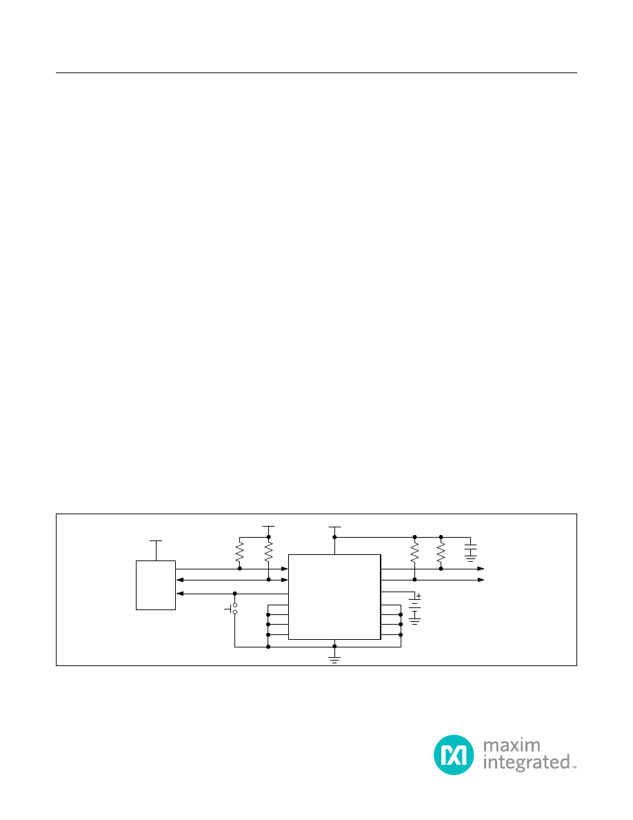
DS3231
V
CC
SCL
R
PU
R
PU
= t
R
/C
B
R
PU
INT
/SQW
32kHz
V
BAT
PUSHBUTTON
RESET
SDA
RST
N.C.
N.C.
N.C.
N.C.
V
CC
V
CC
GND
V
CC
P
N.C.
N.C.
N.C.
N.C.
SCL
SDA
RST
DS3231
Extremely Accurate I
2
C-Integrated
RTC/TCXO/Crystal
Typical Operating Circuit