Siemens simatic S7-1200. Manual (2015) - page 2

PLC concepts made easy
4.4 Memory areas, addressing and data types
Data types
Description
Array and structure
• Array contains multiple elements of the same data type. Arrays can be created in the block
data types
interface editors for OB, FC, FB, and DB. You cannot create an array in the PLC tags editor.
• Struct defines a structure of data consisting of other data types. The Struct data type can be
used to handle a group of related process data as a single data unit. You declare the name
and internal data structure for the Struct data type in the data block editor or a block interface
editor.
Arrays and structures can also be assembled into a larger structure. A structure can be nested
up to eight levels deep. For example, you can create a structure of structures that contain arrays.
PLC data types
PLC Data type is a user-defined data structure that defines a custom data structure that you can
use multiple times in your program. When you create a PLC Data type, the new PLC Data type
appears in the data type selector drop drop-lists in the DB editor and code block interface editor.
PLC Data types can be used directly as a data type in a code block interface or in data blocks.
PLC Data types can be used as a template for the creation of multiple global data blocks that use
the same data structure.
Pointer data types
• Pointer provides an indirect reference to the address of a tag. It occupies 6 bytes (48 bits) in
memory and can include the following information to a variable: DB number (or 0 if the data is
not stored in a DB), memory area in the CPU, and the memory address.
• Any provides an indirect reference to the beginning of a data area and identifies its length.
The Any pointer uses 10 bytes in memory and can include the following information: Data
type of the data elements, number of data elements, memory area or DB number, and the
"Byte.Bit" starting address of the data.
• Variant provides an indirect reference to tags of different data types or parameters. The Vari-
ant pointer recognizes structures and individual structural components. The Variant does not
occupy any space in memory.
Although not available as data types, the following BCD (binary coded decimal) numeric
formats are supported by the conversion instructions.
● BCD16 is a 16-bit value (-999 to 999).
● BCD32 is a 32-bit value (-9999999 to 9999999).
63
PLC concepts made easy
4.4 Memory areas, addressing and data types
4.4.2
Addressing memory areas
STEP 7 facilitates symbolic programming. You create symbolic names or "tags" for the
addresses of the data, whether as PLC tags relating to memory addresses and I/O points or
as local variables used within a code block. To use these tags in your user program, simply
enter the tag name for the instruction parameter. For a better understanding of how the CPU
structures and addresses the memory areas, the following paragraphs explain the "absolute"
addressing that is referenced by the PLC tags. The CPU provides several options for storing
data during the execution of the user program:
● Global memory: The CPU provides a variety of specialized memory areas, including
inputs (I), outputs (Q) and bit memory (M). This memory is accessible by all code blocks
without restriction.
● Data block (DB): You can include DBs in your user program to store data for the code
blocks. The data stored persists when the execution of the associated code block comes
to an end. A "global" DB stores data that can be used by all code blocks, while an
instance DB stores data for a specific FB and is structured by the parameters for the FB.
● Temp memory: Whenever a code block is called, the operating system of the CPU
allocates the temporary, or local, memory (L) to be used during the execution of the
block. When the execution of the code block finishes, the CPU reallocates the local
memory for the execution of other code blocks.
Each different memory location has a unique address. Your user program uses these
addresses to access the information in the memory location.
References to the input (I) or output (Q) memory areas, such as I0.3 or Q1.7, access the
process image. To immediately access the physical input or output, append the reference
with ":P" (such as I0.3:P, Q1.7:P, or "Stop:P").
Forcing applies a fixed value to a physical input (Ix.y:P) or a physical output (Qx.y:P) only.
To force an input or output, append a ":P" to the PLC tag or the address. For more
information, see "Forcing variables in the CPU" (Page 340).
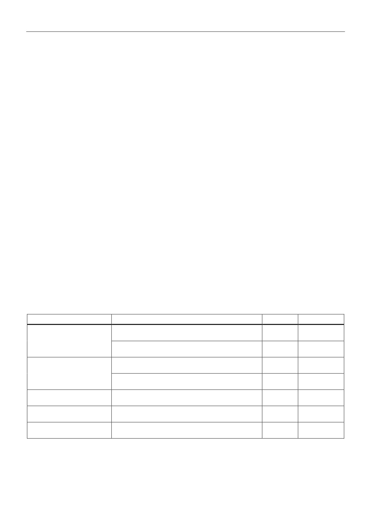
Table 4- 4
Memory areas
Memory area
Description
Force
Retentive
I
Copied from physical inputs at the beginning of the scan
No
No
Process image input
cycle
I_:P1
Immediate read of the physical input points on the CPU,
Yes
No
(Physical input)
SB, and SM
Q
Copied to physical outputs at the beginning of the scan
No
No
Process image output
cycle
Q_:P1
Immediate write to the physical output points on the
Yes
No
(Physical output)
CPU, SB, and SM
M
Control and data memory
No
Yes
Bit memory
(optional)
L
Temporary data for a block local to that block
No
No
Temp memory
DB
Data memory and also parameter memory for FBs
No
Yes
Data block
(optional)
1
To immediately access (or to force) the physical inputs and physical outputs, append a ":P" to the address or tag (such
as I0.3:P, Q1.7:P, or "Stop:P").
64
PLC concepts made easy
4.4 Memory areas, addressing and data types
Each different memory location has a unique address. Your user program uses these
addresses to access the information in the memory location. The absolute address consists
of the following elements:
● Memory area (such as I, Q, or M)
● Size of the data to be accessed (such as "B" for Byte or "W" for Word)
● Address of the data (such as Byte 3 or Word 3)
When accessing a bit in the address for a Boolean value, you do not enter a mnemonic for
the size. You enter only the memory area, the byte location, and the bit location for the data
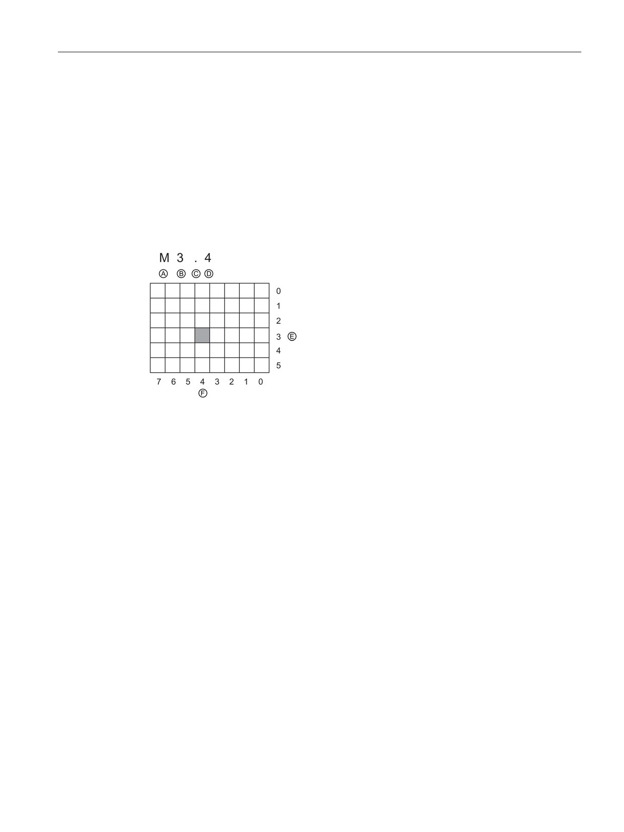
(such as I0.0, Q0.1, or M3.4).
Absolute address of a memory area:
A Memory area identifier
B Byte address: byte 3
C Separator ("byte.bit")
D Bit location of the byte (bit 4 of 8)
E Bytes of the memory area
F Bits of the selected byte
In the example, the memory area and byte address (M = bit memory area, and 3 = Byte 3)
are followed by a period (".") to separate the bit address (bit 4).
65
PLC concepts made easy
4.4 Memory areas, addressing and data types
Configuring the I/O in the CPU and I/O modules
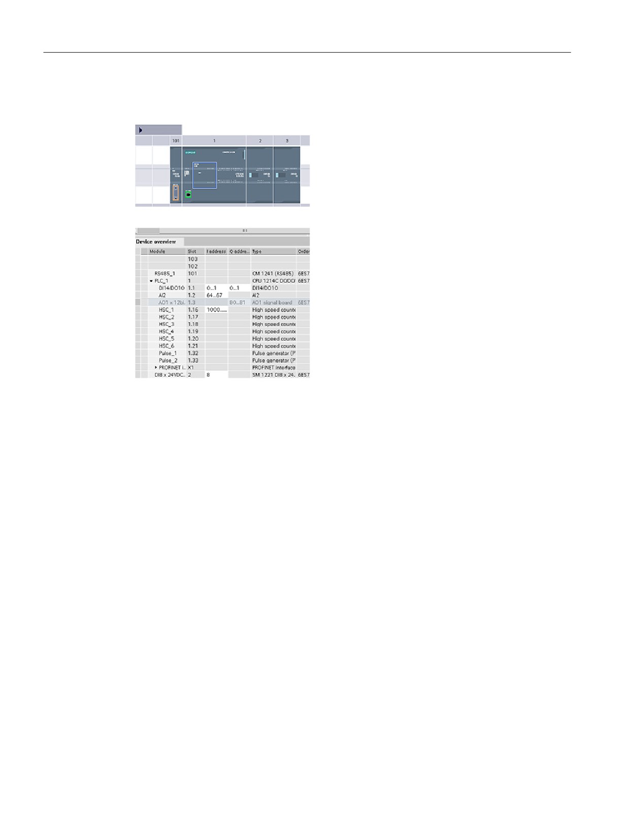
When you add a CPU and I/O modules to your
device configuration, STEP 7 automatically assigns
I and Q addresses. You can change the default
addressing by selecting the address field in the
device configuration and entering new numbers.
• STEP 7 assigns digital inputs and outputs in
groups of 8 points (1 byte), whether the module
uses all the points or not.
• STEP 7 allocates analog inputs and outputs in
groups of 2, where each analog poing occupies
2 bytes (16 bits).
The figure shows an example of a CPU 1214C with two SMs and one SB. In this example,
you could change the address of the DI8 module to 2 instead of 8. The tool assists you by
changing address ranges that are the wrong size or conflict with other addresses.
66
PLC concepts made easy
4.4 Memory areas, addressing and data types
4.4.3
Accessing a "slice" of a tagged data type
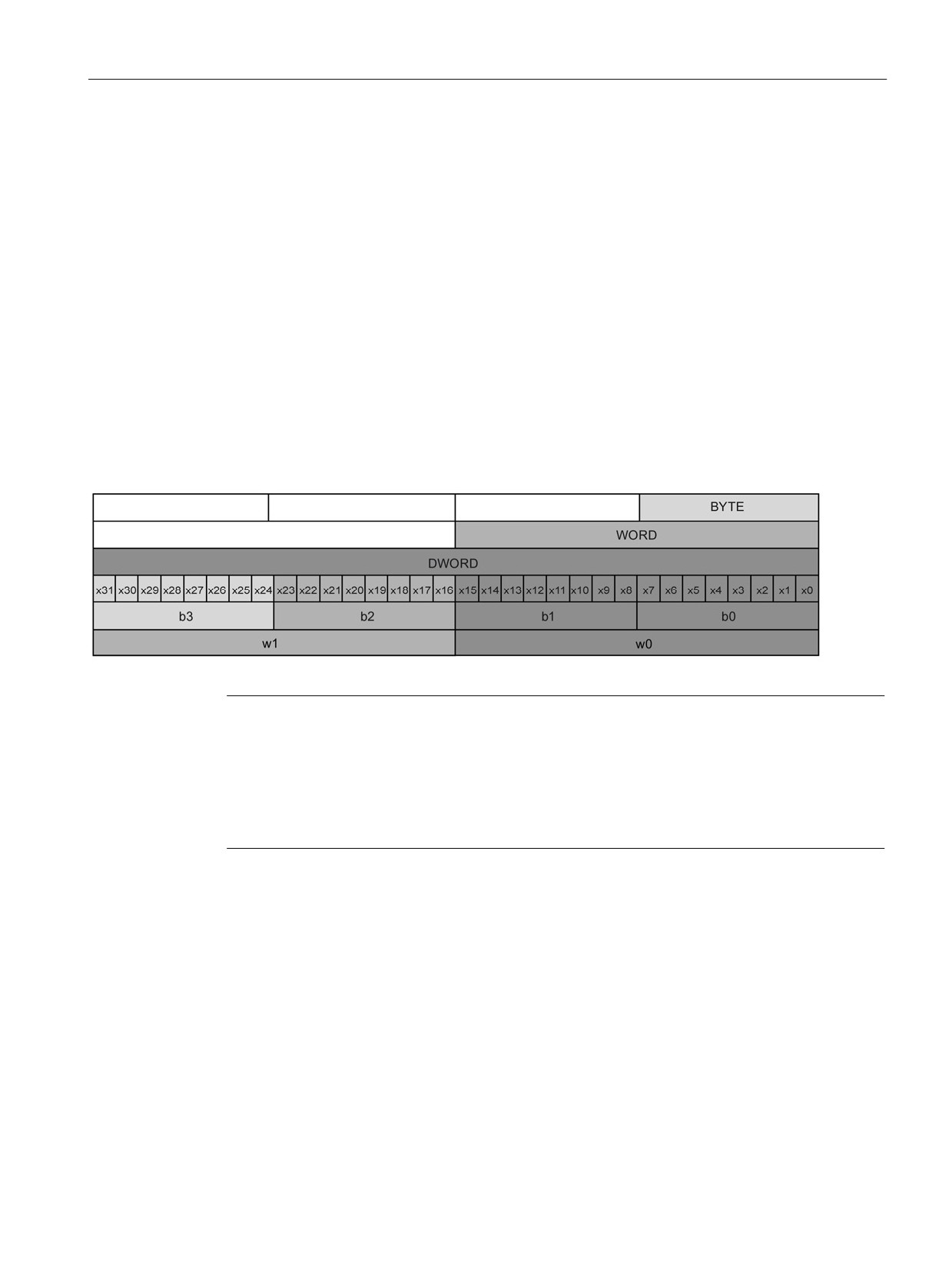
PLC tags and data block tags can be accessed at the bit, byte, or word level depending on
their size. The syntax for accessing such a data slice is as follows:
● "<PLC tag name>".xn (bit access)
● "<PLC tag name>".bn (byte access)
● "<PLC tag name>".wn (word access)
● "<Data block name>".<tag name>.xn (bit access)
● "<Data block name>".<tag name>.bn (byte access)
● "<Data block name>".<tag name>.wn (word access)
A double word-sized tag can be accessed by bits 0 - 31, bytes 0 - 3, or word 0 - 1. A word-
sized tag can be accessed by bits 0 - 15, bytes 0 - 1, or word 0. A byte-sized tag can be
accessed by bits 0 - 7, or byte 0. Bit, byte, and word slices can be used anywhere that bits,
bytes, or words are expected operands.
Note
Valid data types that can be accessed by slice are Byte, Char, Conn_Any, Date, DInt,
DWord, Event_Any, Event_Att, Hw_Any, Hw_Device, HW_Interface, Hw_Io, Hw_Pwm,
Hw_SubModule, Int, OB_Any, OB_Att, OB_Cyclic, OB_Delay, OB_WHINT, OB_PCYCLE,
OB_STARTUP, OB_TIMEERROR, OB_Tod, Port, Rtm, SInt, Time, Time_Of_Day, UDInt,
UInt, USInt, and Word. PLC Tags of type Real can be accessed by slice, but data block tags
of type Real cannot.
67
PLC concepts made easy
4.4 Memory areas, addressing and data types
Examples
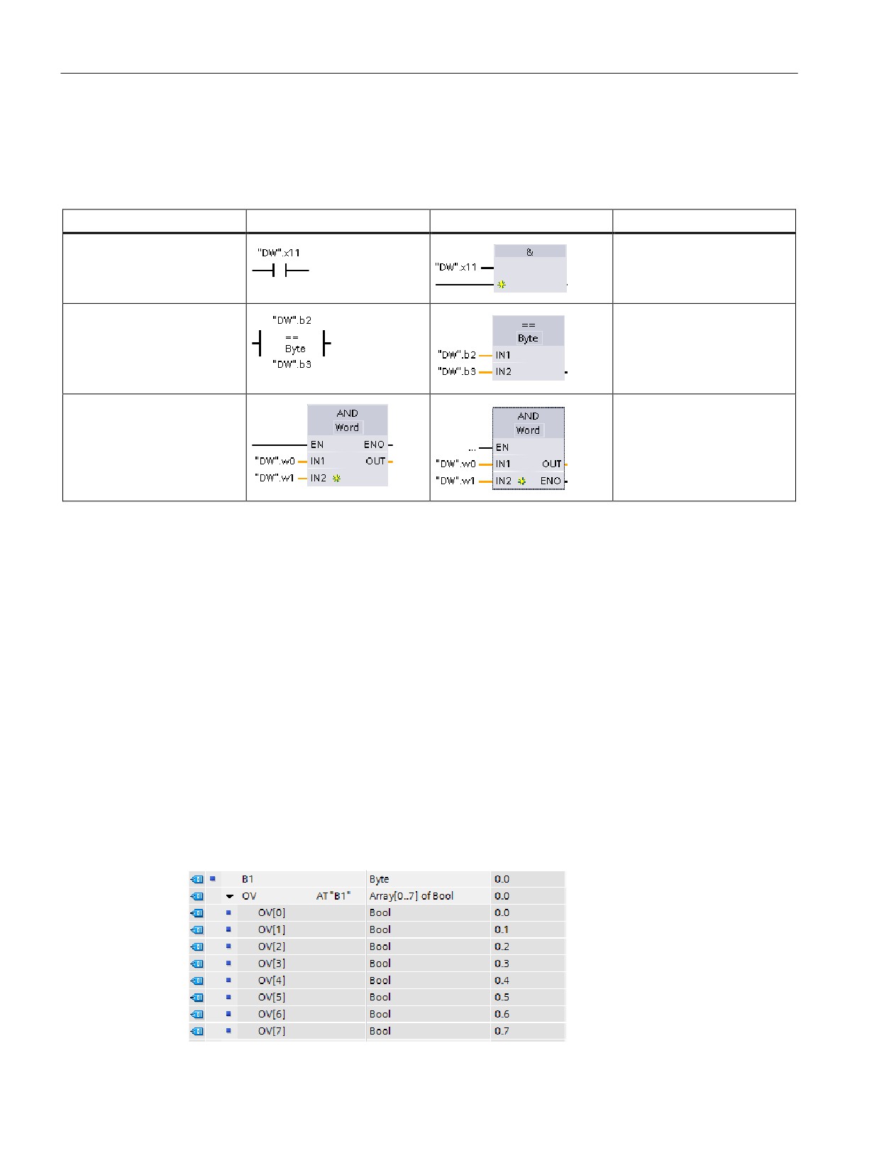
In the PLC tag table, "DW" is a declared tag of type DWORD. The examples show bit, byte,
and word slice access:
LAD
FBD
SCL
Bit access
IF "DW".x11 THEN
END_IF;
Byte access
IF "DW".b2 = "DW".b3
THEN
END_IF;
Word access
out:= "DW".w0 AND
"DW".w1;
4.4.4
Accessing a tag with an AT overlay
The AT tag overlay allows you to access an already-declared tag of a standard access block
with an overlaid declaration of a different data type. You can, for example, address the
individual bits of a tag of a Byte, Word, or DWord data type with an Array of Bool.
Declaration
To overlay a parameter, declare an additional parameter directly after the parameter that is
to be overlaid and select the data type "AT". The editor creates the overlay, and you can
then choose the data type, struct, or array that you wish to use for the overlay.
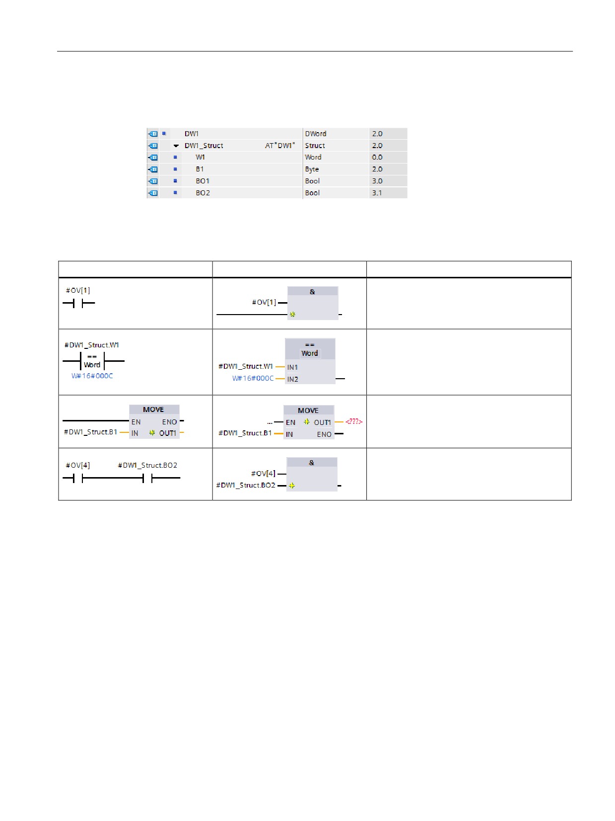
Example
This example shows the input parameters of a standard-access FB. The byte tag B1 is
overlaid with an array of Booleans:
68
PLC concepts made easy
4.4 Memory areas, addressing and data types
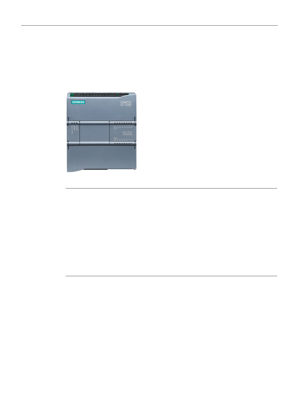
Another example is a DWord tag overlaid with a Struct, which includes a Word, Byte, and
two Booleans:
The Offset column of the block interface shows the location of the overlaid data types
relative to the original tag.
You can addresss the overlay types directly in the program logic:
LAD
FBD
SCL
IF #OV[1] THEN
END_IF;
IF #DW1_Struct.W1 = W#16#000C THEN
END_IF;
out1 := #DW1_Struct.B1;
IF #OV[4] AND #DW1_Struct.BO2 THEN
END_IF;
Rules
● Overlaying of tags is only possible in FB and FC blocks with standard (not optimized)
access.
● You can overlay parameters for all block types and all declaration sections.
● You can use an overlaid parameter like any other block parameter.
● You cannot overlay parameters of type VARIANT.
● The size of the overlaying parameter must be less than or equal to the size of the overlaid
parameter.
● You must declare the overlaying variable immediately after the variable that it overlays
and select the keyword "AT" as the initial data type selection.
69
PLC concepts made easy
4.5 Pulse outputs
4.5
Pulse outputs
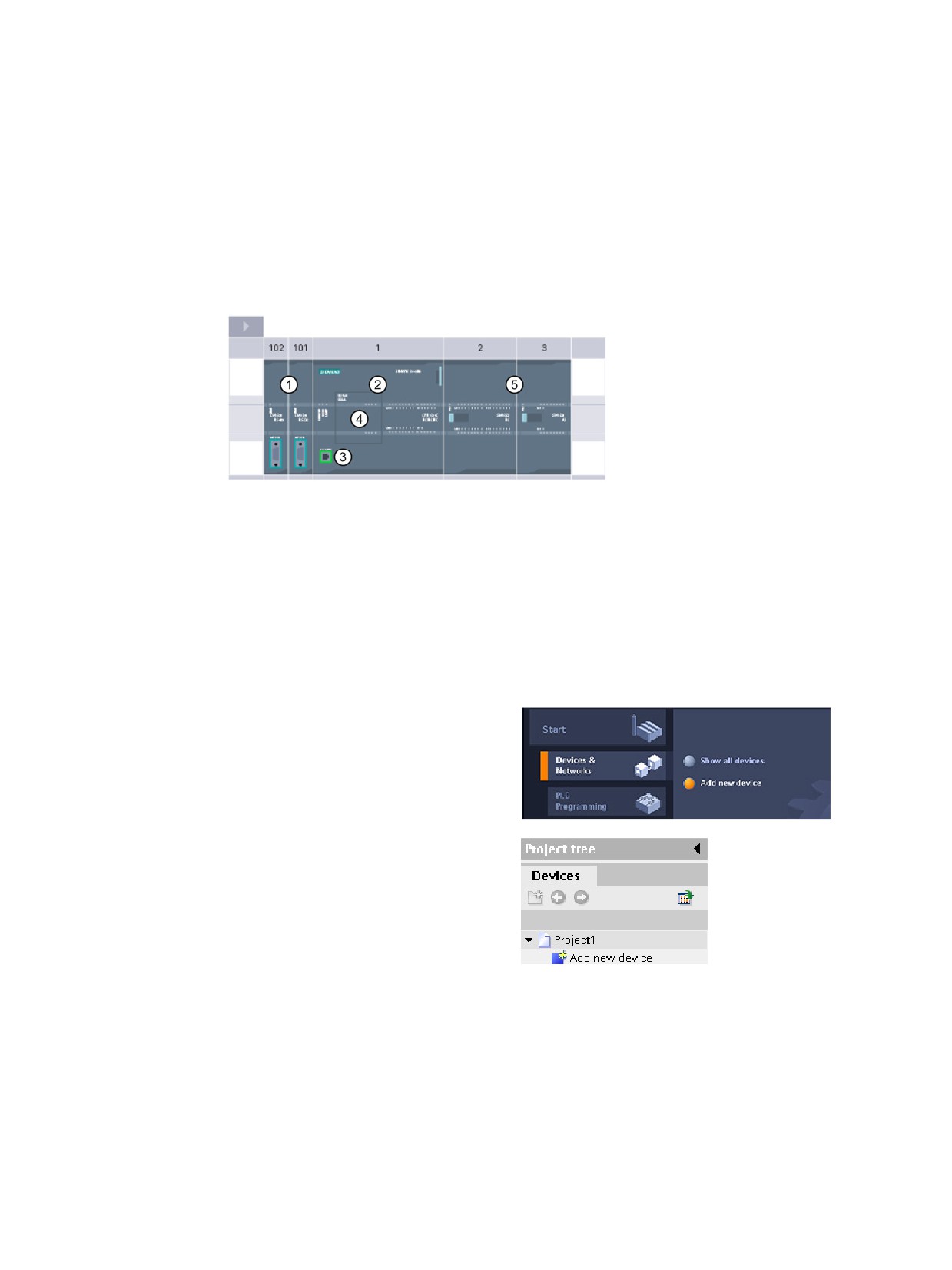
The CPU or signal board (SB) can be configured to provide four pulse generators for
controlling high-speed pulse output functions, either as pulse-width modulation (PWM) or as
pulse-train output (PTO). The basic motion instructions use PTO outputs. You can assign
each pulse generator to either PWM or PTO, but not both at the same time.
Pulse outputs cannot be used by other instructions in the
user program. When you configure the outputs of the
CPU or SB as pulse generators, the corresponding out-
put addresses are removed from the Q memory and can-
not be used for other purposes in your user program. If
your user program writes a value to an output used as a
pulse generator, the CPU does not write that value to the
physical output.
Note
Do not exceed the maximum pulse frequency.
The maximum pulse frequency of the pulse output generators is 1 MHz for the CPU 1217C
and 100 kHz for CPUs 1211C, 1212C, 1214C, and 1215C; 20 kHz (for a standard SB); or
200 kHz (for a high-speed SB).
The four pulse generators have default I/O assignments; however, they can be configured to
any digital output on the CPU or SB. Pulse generators on the CPU cannot be assigned to
distributed I/O.
When configuring the basic motion instructions, be aware that STEP 7 does not alert you if
you configure an axis with a maximum speed or frequency that exceeds this hardware
limitation. This could cause problems with your application, so always ensure that you do not
exceed the maximum pulse frequency of the hardware.
You can use onboard CPU outputs, or you can use the optional signal board outputs. The
output point numbers are shown in the following table (assuming the default output
configuration). If you have changed the output point numbering, then the output point
numbers will be those you assigned. Note that PWM requires only one output, while PTO
can optionally use two outputs per channel. If an output is not required for a pulse function, it
is available for other uses.
70

PLC concepts made easy
4.5 Pulse outputs
The four pulse generators have default I/O assignments; however, they can be configured to
any digital output on the CPU or SB. Pulse generators on the CPU cannot be assigned to
SMs or to distributed I/O.
Table 4- 5
Default output assignments for the pulse generators
Description
Pulse
Direction
PTO1
Built-in I/O
Q0.0
Q0.1
SB I/O
Q4.0
Q4.1
PWM1
Built-in outputs
Q0.0
-
SB outputs
Q4.0
-
PTO2
Built-in I/O
Q0.2
Q0.3
SB I/O
Q4.2
Q4.3
PWM2
Built-in outputs
Q0.2
-
SB outputs
Q4.2
-
PTO3
Built-in I/O
Q0.41
Q0.51
SB I/O
Q4.0
Q4.1
PWM3
Built-in outputs
Q0.41
-
SB outputs
Q4.1
-
PTO4
Built-in I/O
Q0.62
Q0.72
SB I/O
Q4.2
Q4.3
PWM4
Built-in outputs
Q0.62
-
SB outputs
Q4.3
-
1
The CPU 1211C does not have outputs Q0.4, Q0.5, Q0.6, or Q0.7. Therefore, these outputs can-
not be used in the CPU 1211C.
2
The CPU 1212C does not have outputs Q0.6 or Q0.7. Therefore, these outputs cannot be used in
the CPU 1212C.
3
This table applies to the CPU 1211C, CPU 1212C, CPU 1214C, CPU 1215C, and CPU 1217C
PTO/PWM functions.
71
PLC concepts made easy
4.5 Pulse outputs
72
Easy to create the device configuration
5
You create the device configuration for your PLC by adding a CPU and additional modules to
your project.
① Communications module (CM) or communication processor (CP): Up to 3, inserted in slots
101, 102, and 103
② CPU: Slot 1
③ Ethernet port of CPU
④ Signal board (SB), communication board (CB) or battery board (BB): up to 1, inserted in the
CPU
⑤ Signal module (SM) for digital or analog I/O: up to 8, inserted in slots 2 through 9
(CPU 1214C, CPU 1215C and CPU 1217C allow 8, CPU 1212C allows 2, CPU 1211C does
not allow any)
To create the device configuration, add a
device to your project.
• In the Portal view, select "Devices &
Networks" and click "Add device".
• In the Project view, under the project
name, double-click "Add new device".
73
Easy to create the device configuration
5.1 Uploading the configuration of a connected CPU
5.1
Uploading the configuration of a connected CPU
STEP 7 provides two methods for uploading the hardware configuration of a connected
CPU:
● Uploading the connected device as a new station
● Configuring an unspecified CPU and detecting the hardware configuration of the
connected CPU
Note, however, that the first method uploads both the hardware configuration and the
software of the connected CPU.
Uploading a device as a new station
To upload a connected device as a new station, follow these steps:
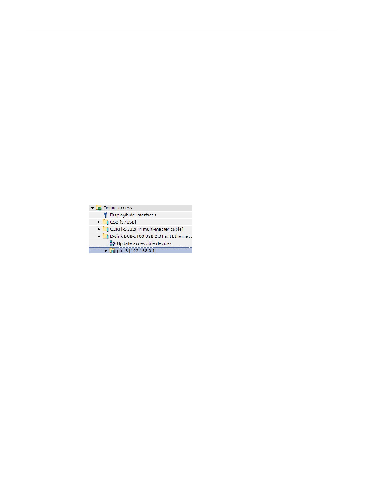
1. Expand your communications interface from the "Online access" node of the project tree.
2. Double-click "Update accessible devices".
3. Select the PLC from the detected devices.
4. From the Online menu of STEP 7, select the "Upload device as new station (hardware
and software)" menu command.
STEP 7 uploads both the hardware configuration and the program blocks.
74
Easy to create the device configuration
5.1 Uploading the configuration of a connected CPU
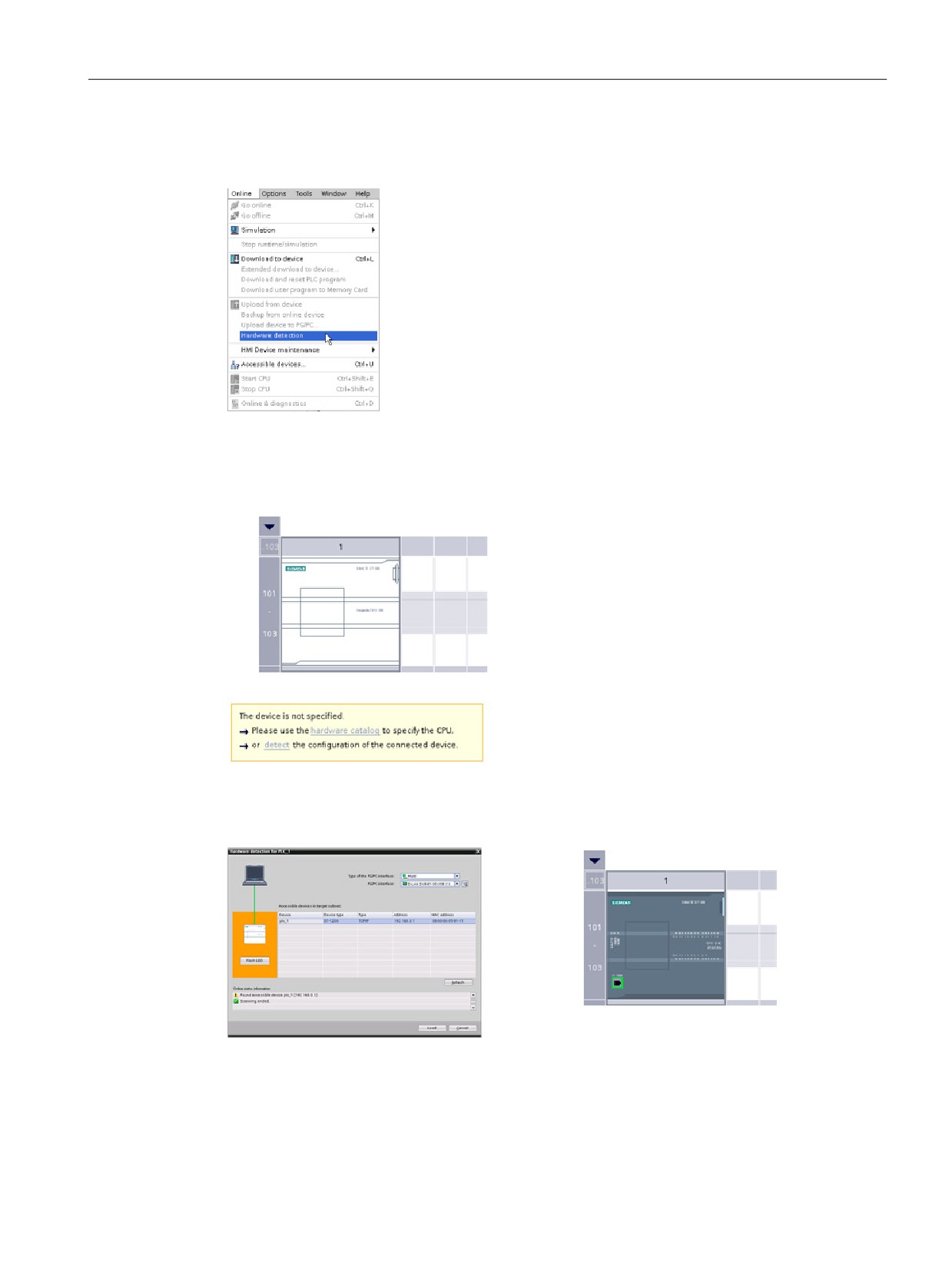
Detecting the hardware configuration of an unspecified CPU
If you are connected to a CPU, you can upload the
configuration of that CPU, including any modules, to
your project. Simply create a new project and select
the "unspecified CPU" instead of selecting a specific
CPU. (You can also skip the device configuration en-
tirely by selecting the "Create a PLC program" from the
"First steps". STEP 7 then automatically creates an
unspecified CPU.)
From the program editor, you select the "Hardware
detection" command from the "Online" menu.
From the device configuration editor, you select the option for detecting the configuration of
the connected device.
After you select the CPU from the online dialog and click the Load button, STEP 7 uploads
the hardware configuration from the CPU, including any modules (SM, SB, or CM). You can
then configure the parameters for the CPU and the modules (Page 80).
75
Easy to create the device configuration
5.2 Adding a CPU to the configuration
5.2
Adding a CPU to the configuration
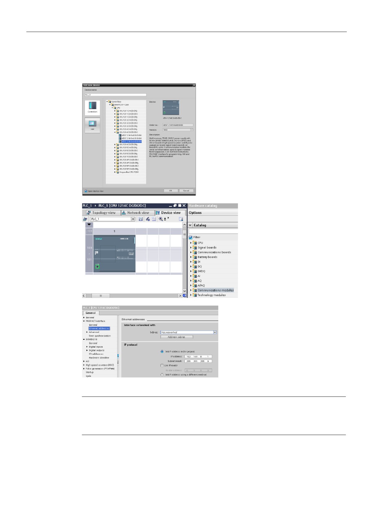
You create your device configuration by inserting
a CPU into your project. Select the CPU in the
"Add a new device" dialog and click "OK" to add
the CPU to the project.
The Device view shows the
CPU and rack.
Selecting the CPU in the Device view
displays the CPU properties in the in-
spector window. Use these properties to
configure the operational parameters of
the CPU (Page 80).
Note
The CPU does not have a pre-configured IP address. You must manually assign an IP
address for the CPU during the device configuration. If your CPU is connected to a router on
the network, you also enter the IP address for a router.
76
Easy to create the device configuration
5.3 Changing a device
5.3
Changing a device
You can change the device type of a configured CPU or module. From Device configuration,
right-click the device and select "Change device" from the context menu. From the dialog,
navigate to and select the CPU or module that you want to replace. The Change device
dialog shows you compatibility information between the two devices.
Note
Device exchange: replacing a V3.0 CPU with a V4.1 CPU
You can open a STEP 7 V12 project in STEP 7 V13 and replace V3.0 CPUs with V4.1
CPUs. You cannot replace CPUs that are from versions prior to V3.0. When you replace a
V3.0 CPU with a V4.1 CPU, consider the differences (Page 433) in features and behavior
between the two versions, and actions you must take.
If you have a project for a CPU version older than V3.0, you must first upgrade the CPU to
V3.0 and then upgrade it to V4.1.
77
Easy to create the device configuration
5.4 Adding modules to the configuration
5.4
Adding modules to the configuration
Use the hardware catalog to add modules to the CPU:
● Signal module (SM) provides additional digital or analog I/O points. These modules are
connected to the right side of the CPU.
● Signal board (SB) provides just a few additional I/O points for the CPU. The SB is
installed on the front of the CPU.
● Battery Board 1297 (BB) provides long-term backup of the realtime clock. The BB is
installed on the front of the CPU.
● Communication board (CB) provides an additional communication port (such as RS485).
The CB is installed on the front of the CPU.
● Communication module (CM) and communication processor (CP) provide an additional
communication port, such as for PROFIBUS or GPRS. These modules are connected to
the left side of the CPU.
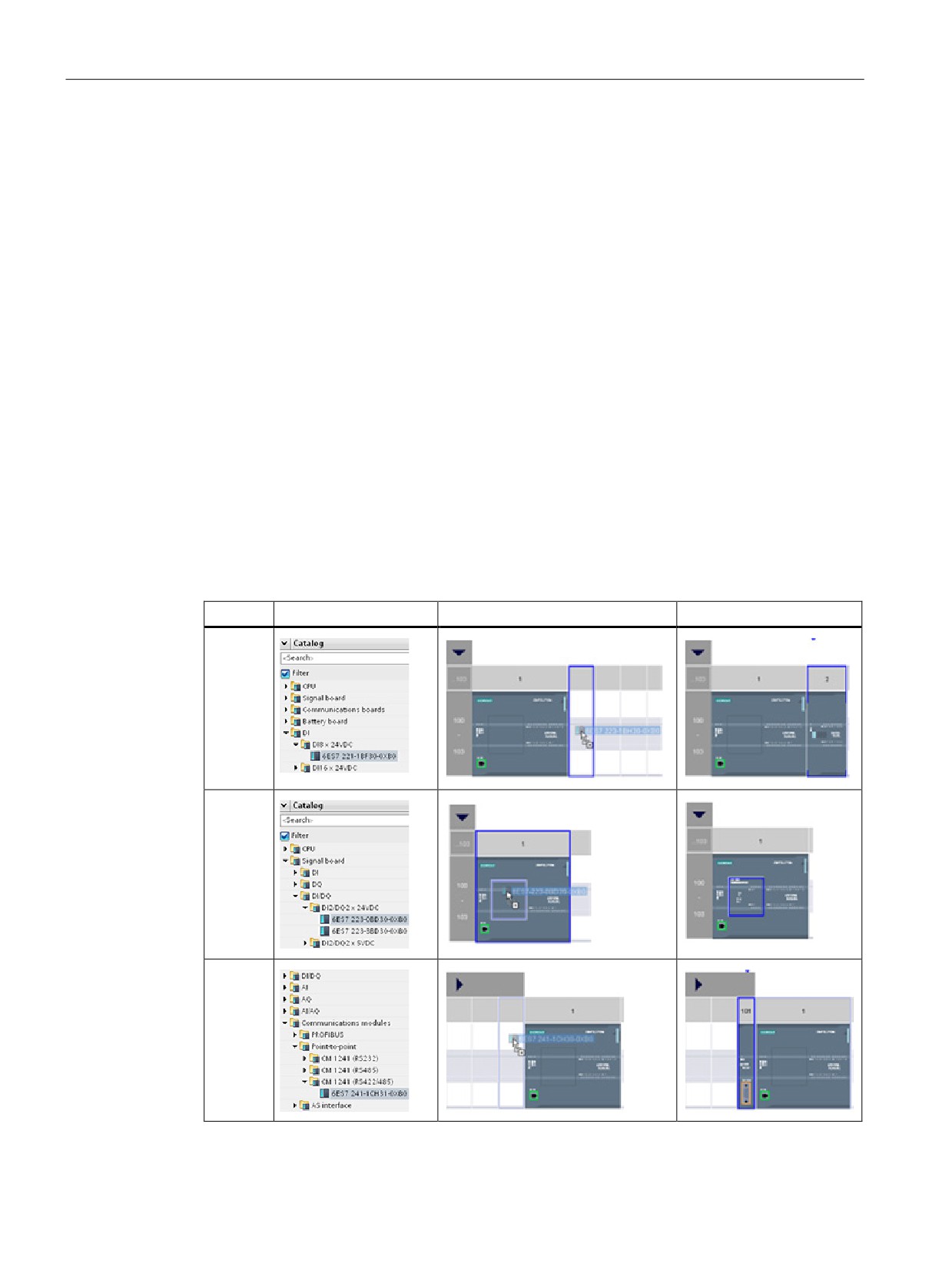
To insert a module into the device configuration, select the module in the hardware catalog
and either double-click or drag the module to the highlighted slot. You must add the modules
to the device configuration and download the hardware configuration to the CPU for the
modules to be functional.
Table 5- 1
Adding a module to the device configuration
Module
Select the module
Insert the module
Result
SM
SB, BB
or CB
CM or
CP
78
Easy to create the device configuration
5.5 Configuration control
With the "configuration control" feature (Page 79), you can add signal modules and signal
boards to your device configuration that might not correspond to the actual hardware for a
specific application, but that will be used in related applications that share a common user
program, CPU model, and perhaps some of the configured modules.
5.5
Configuration control
Configuration control can be a useful solution when you create an automation solution
(machine) that you intend to use with variations in multiple installations.
Configuration control with STEP 7 and the S7-1200 enables you to configure a maximum
configuration for a standard machine and to operate versions (options) that use a subset of
this configuration. The PROFINET with STEP 7 manual
projects as "standard machine projects".
You can load a STEP 7 device configuration and user program to different installed PLC
configurations. You only need to make a few easy adaptations to make the STEP 7 project
correspond to the actual installation.
A control data record that you program in the startup program block notifies the CPU as to
which modules are missing in the real installation as compared to the configuration or which
modules are located in different slots as compared to the configuration. Configuration control
does not have an impact on the parameter assignment of the modules.
Configuration control gives you the flexibility to vary the installation as long as you can derive
the real configuration from the maximum device configuration in STEP 7.
You can find instructions and examples for configuration control in the S7-1200
Programmable Controller System Manual.
79
Easy to create the device configuration
5.6 Configuring the operation of the CPU and modules
5.6
Configuring the operation of the CPU and modules
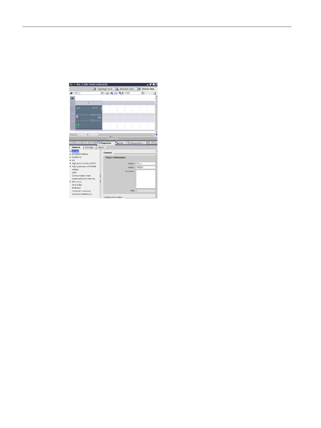
To configure the operational parameters for the CPU, select the CPU in the Device view and
use the "Properties" tab of the inspector window.
You can configure the following CPU properties:
• PROFINET IP address and time
synchronization for the CPU
• Startup behavior of the CPU following an OFF-
to-ON power transition
• Local (on-board) digital and analog I/O, high-
speed counters (HSC), and pulse generators
• System clock (time, time zone and daylight
saving time)
• Read/write protection and password for
accessing the CPU
• Maximum cycle time or a fixed minimum cycle
time and communications load
• Web server properties
Configuring the STOP-to-RUN operation of the CPU
Whenever the operating state changes from STOP to RUN, the CPU clears the process
image inputs, initializes the process image outputs, and processes the startup OBs.
(Therefore, any read accesses to the process-image inputs by instructions in the startup OBs
will read zero rather than the current physical input value.) To read the current state of a
physical input during startup, you must perform an immediate read. The startup OBs and any
associated FCs and FBs are executed next. If more than one startup OB exists, each is
executed in order according to the OB number, with the lowest OB number executing first.
The CPU also performs the following tasks during the startup processing.
● Interrupts are queued but not processed during the startup phase
● No cycle time monitoring is performed during the startup phase
● Configuration changes to HSC (high-speed counter), PWM (pulse-width modulation), and
PtP (point-to-point communication) modules can be made in startup
● Actual operation of HSC, PWM, and point-to-point communication modules only occurs in
RUN
After the execution of the startup OBs finishes, the CPU goes to RUN mode and processes
the control tasks in a continuous scan cycle.
80
Easy to create the device configuration
5.6 Configuring the operation of the CPU and modules
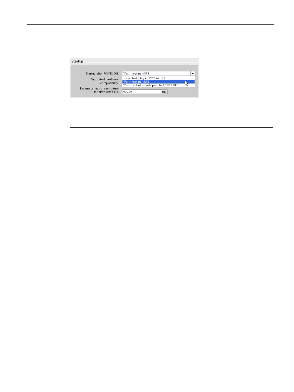
Use the CPU properties to configure how the CPU starts up after a power cycle.
• In STOP mode
• In RUN mode
• In the previous
mode (prior to the
power cycle)
The CPU performs a warm restart before going to RUN mode. Warm restart resets all non-
retentive memory to the default start values, but the CPU retains the current values stored in
the retentive memory.
Note
The CPU always performs a restart after a download
Whenever you download an element of your project (such as a program block, data block, or
hardware configuration), the CPU performs a restart on the next transition to RUN mode. In
addition to clearing the inputs, initializing the outputs and initializing the non-retentive
memory, the restart also initializes the retentive memory areas.
After the restart that follows a download, all subsequent STOP-to-RUN transitions perform a
warm restart (that does not initialize the retentive memory).
81
Easy to create the device configuration
5.6 Configuring the operation of the CPU and modules
5.6.1
System memory and clock memory provide standard functionality
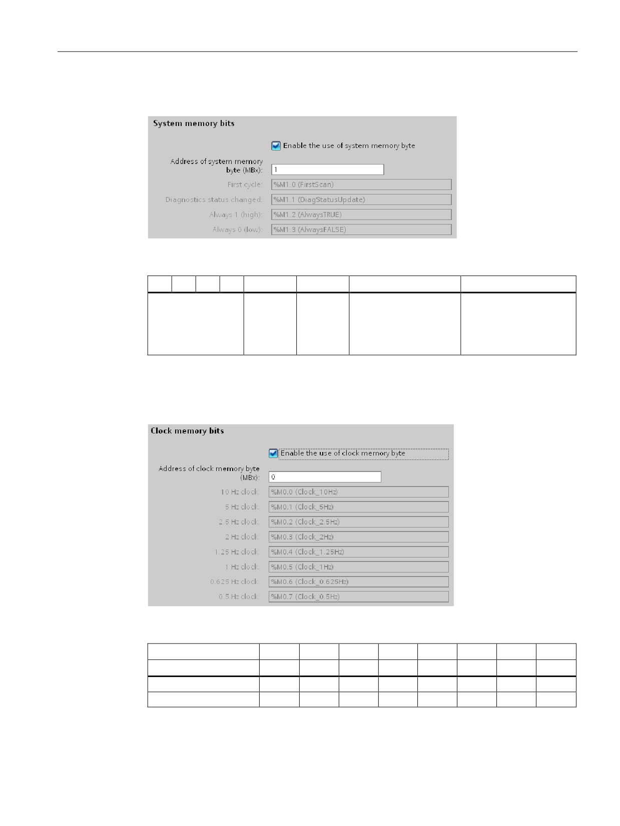
You use the CPU properties to enable bytes for "system memory" and "clock memory". Your
program logic can reference the individual bits of these functions by their tag names.
● You can assign one byte in M memory for system memory. The byte of system memory
provides the following four bits that can be referenced by your user program by the
following tag names:
- First cycle: (Tag name "FirstScan") bit is set to1 for the duration of the first scan after
the startup OB finishes. (After the execution of the first scan, the "first scan" bit is set
to 0.)
- Diagnostics status changed: (Tag name: "DiagStatusUpdate") is set to 1 for one scan
after the CPU logs a diagnostic event. Because the CPU does not set the
"DiagStatusUpdate" bit until the end of the first execution of the program cycle OBs,
your user program cannot detect if there has been a diagnostic change either during
the execution of the startup OBs or the first execution of the program cycle OBs.
- Always 1 (high): (Tag name "AlwaysTRUE") bit is always set to 1.
- Always 0 (low): (Tag name "AlwaysFALSE") bit is always set to 0.
● You can assign one byte in M memory for clock memory. Each bit of the byte configured
as clock memory generates a square wave pulse. The byte of clock memory provides 8
different frequencies, from 0.5 Hz (slow) to 10 Hz (fast). You can use these bits as control
bits, especially when combined with edge instructions, to trigger actions in the user
program on a cyclic basis.
The CPU initializes these bytes on the transition from STOP mode to STARTUP mode. The
bits of the clock memory change synchronously to the CPU clock throughout the STARTUP
and RUN modes.
CAUTION
Risks with overwriting the system memory or clock memory bits
Overwriting the system memory or clock memory bits can corrupt the data in these
functions and cause your user program to operate incorrectly, which can cause damage to
equipment and injury to personnel.
Because both the clock memory and system memory are unreserved in M memory,
instructions or communications can write to these locations and corrupt the data.
Avoid writing data to these locations to ensure the proper operation of these functions, and
always implement an emergency stop circuit for your process or machine.
82
Easy to create the device configuration
5.6 Configuring the operation of the CPU and modules
System memory configures a byte with bits that turn on (value = 1) for a specific event.
Table 5- 2
System memory
7
6
5
4
3
2
1
0
Reserved
Always off
Always on
Diagnostic status indica-
First scan indicator
tor
Value 0
Value 0
Value 1
•
1: First scan after
•
1: Change
startup
•
0: No change
•
0: Not first scan
Clock memory configures a byte that cycles the individual bits on and off at fixed intervals.
Each clock bit generates a square wave pulse on the corresponding M memory bit. These
bits can be used as control bits, especially when combined with edge instructions, to trigger
actions in the user code on a cyclic basis.
Table 5- 3
Clock memory
Bit number
7
6
5
4
3
2
1
0
Tag name
Period (s)
2.0
1.6
1.0
0.8
0.5
0.4
0.2
0.1
Frequency (Hz)
0.5
0.625
1
1.25
2
2.5
5
10
Because clock memory runs asynchronously to the CPU cycle, the status of the clock memory can
change several times during a long cycle.
83
Easy to create the device configuration
5.6 Configuring the operation of the CPU and modules
Configuring the operation of the I/O and communication modules
To configure the operational parameters for the signal module (SM), signal board (SB), or
communication module (CM), select the module in the Device view and use the "Properties"
tab of the inspector window.
Signal module (SM) and signal board (SB)
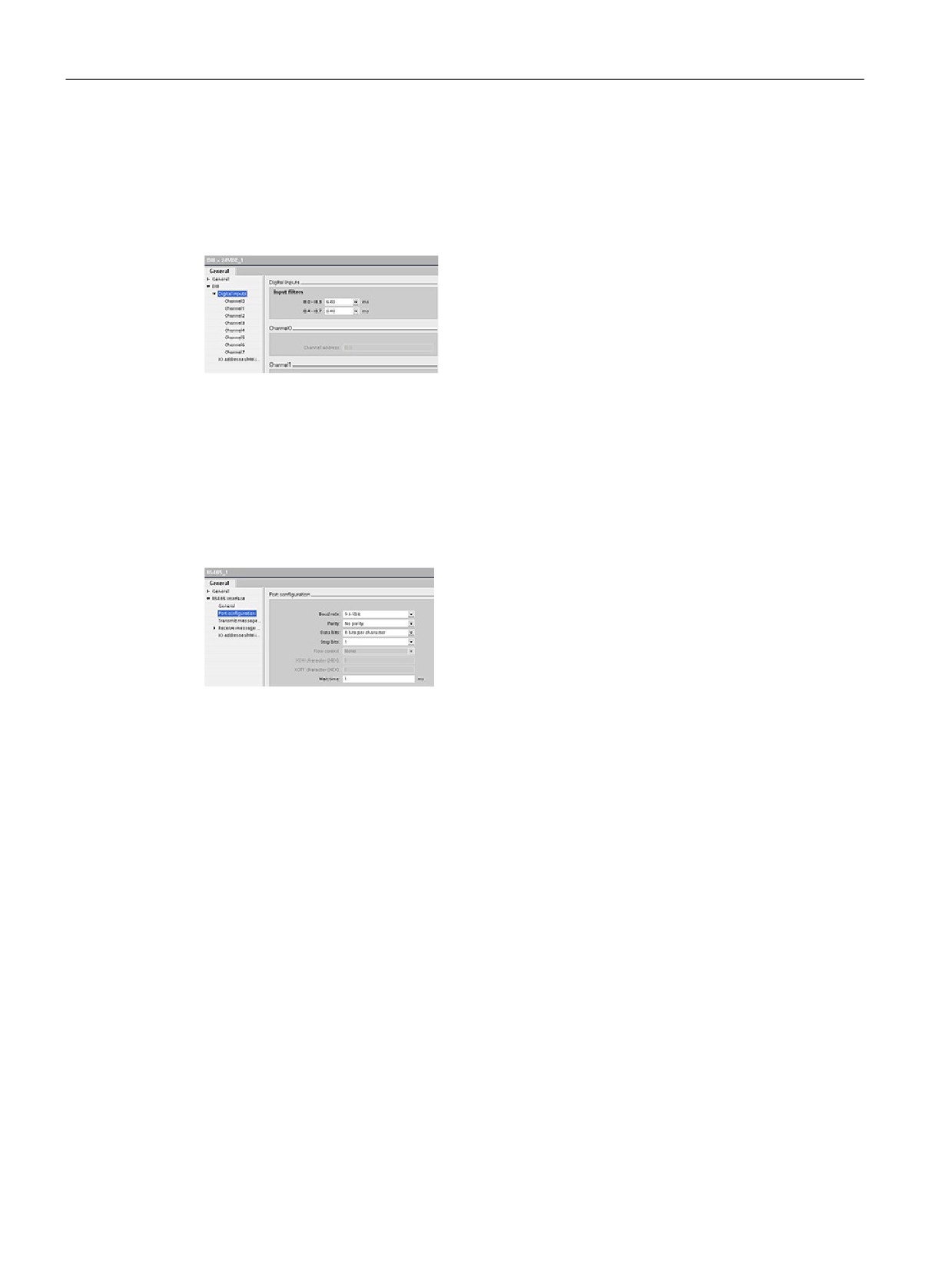
• Digital I/O: Configure the individual inputs, such as
for Edge detection and "pulse catch" (to stay on or
off for one scan after a momentary high- or low
pulse). Configure the outputs to use a freeze or
substitute value on a transition from RUN mode to
STOP mode.
● Analog I/O: Configure the parameters for individual inputs (such as voltage / current,
range and smoothing) and also enable underflow or overflow diagnostics. Configure the
parameters for individual analog outputs and enable diagnostics, such as short-circuit (for
voltage outputs) or overflow values.
● I/O addresses: Configure the start address for the set of inputs and outputs of the
module.
Communication module (CM) and communication
board (CB)
• Port configuration: Configure the communication
parameters, such as baud rate, parity, data bits,
stop bits, and wait time.
● Transmit and receive message: Configure options related to transmitting and receiving
data (such as the message-start and message-end parameters)
You can also change these configuration parameters with your user program.
84
Easy to create the device configuration
5.7 Configuring the IP address of the CPU
5.7
Configuring the IP address of the CPU
Because the CPU does not have a pre-configured IP address, you must manually assign an
IP address. You configure the IP address and the other parameters for the PROFINET
interface when you configure the properties for the CPU.
● In a PROFINET network, each device is assigned a unique Media Access Control
address (MAC address) by the manufacturer for identification. Each device must also
have an IP address.
● A subnet is a logical grouping of connected network devices. A mask (also known as the
subnet mask or network mask) defines the boundaries of a subnet. The only connection
between different subnets is via a router. Routers are the link between LANs and rely on
IP addresses to deliver and receive data packets.
Before you can download an IP address to the CPU, you must ensure that the IP address for
your CPU is compatible with the IP address of your programming device.
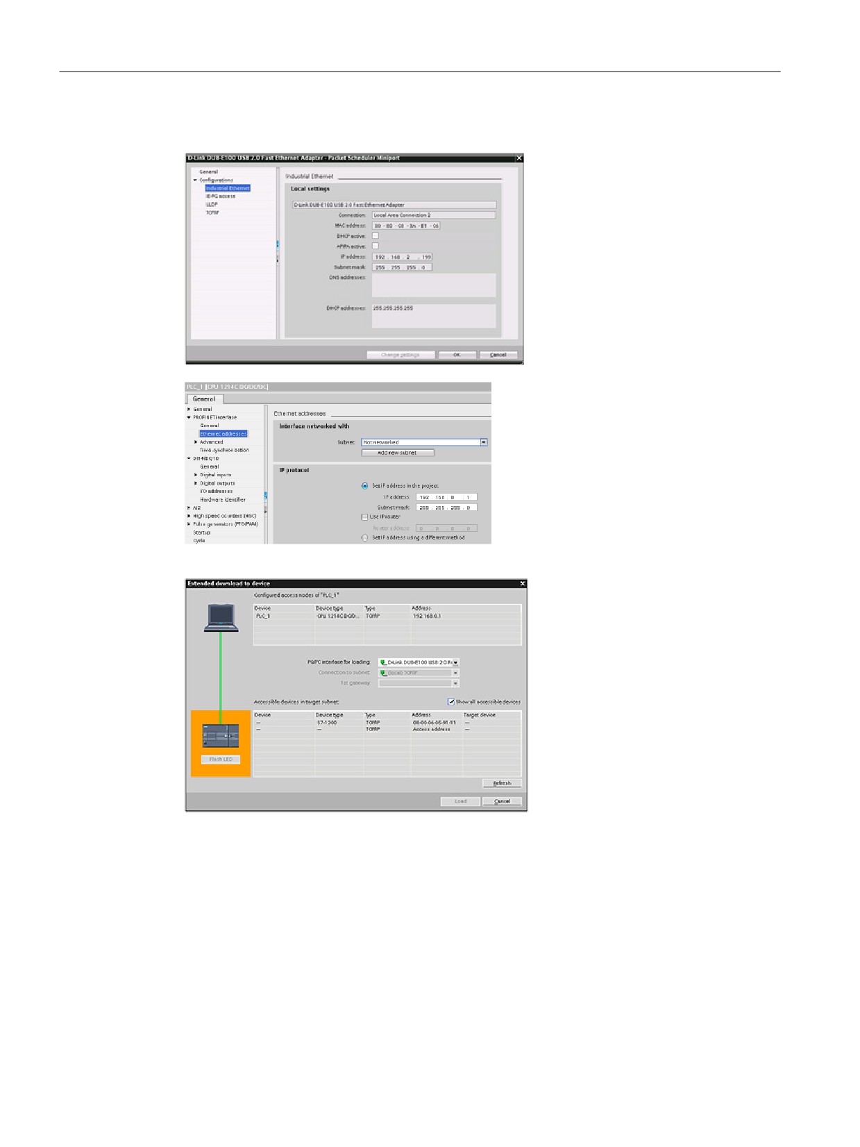
You can use STEP 7 to determine the IP address of your programming device:
1. Expand the "Online access" folder in the Project tree to display your networks.
2. Select the network that connects to the CPU.
3. Right-click the specific network to display the context menu.
4. Select the "Properties" command.
Note
The IP address for the CPU must be compatible with the IP address and subnet mask for
the programming device. Consult your network specialist for a suitable IP address and
subnet mask for your CPU.
85
Easy to create the device configuration
5.7 Configuring the IP address of the CPU
The "Properties" window displays
the settings for the programming
device.
After determining the IP address
and subnet mask for the CPU,
enter the IP address for the CPU
and for the router (if applicable).
Refer to the S7-1200 Program-
mable Controller System Manual
for more information.
After completing the configuration,
download the project to the CPU.
The IP addresses for the CPU and
for the router (if applicable) are con-
figured when you download the
project.
86
Easy to create the device configuration
5.8 Protecting access to the CPU or code block is easy
5.8
Protecting access to the CPU or code block is easy
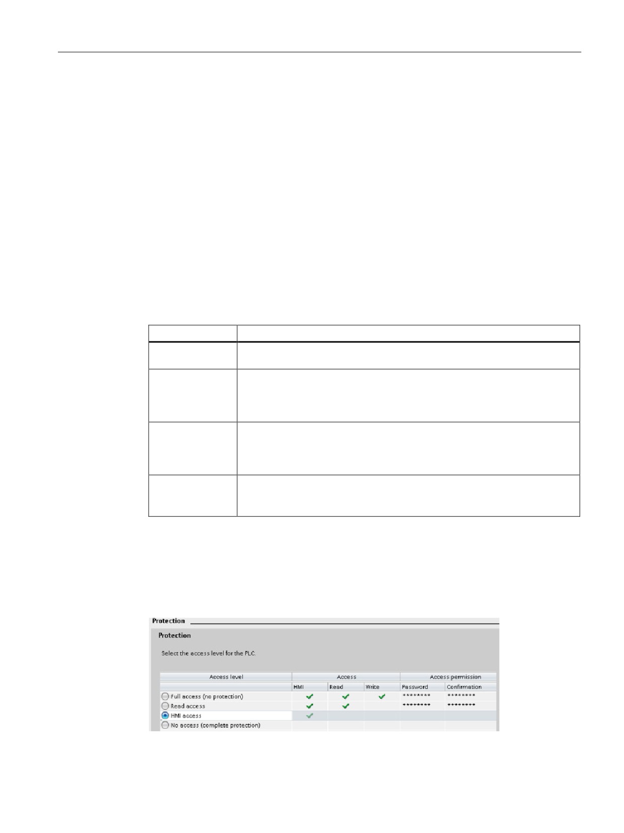
The CPU provides four levels of security for restricting access to specific functions. When
you configure the security level and password for a CPU, you limit the functions and memory
areas that can be accessed without entering a password.
Each level allows certain functions to be accessible without a password. The default
condition for the CPU is to have no restriction and no password-protection. To restrict access
to a CPU, you configure the properties of the CPU and enter the password.
Entering the password over a network does not compromise the password protection for the
CPU. Password protection does not apply to the execution of user program instructions
including communication functions. Entering the correct password provides access to all of
the functions at that level.
PLC-to-PLC communications (using communication instructions in the code blocks) are not
restricted by the security level in the CPU.
Table 5- 4
Security levels for the CPU
Security level
Access restrictions
Full access (no
Allows full access without password protection.
protection)
Read access
Allows HMI access and all forms of PLC-to-PLC communications without pass-
word protection.
Password is required for modifying (writing to) the CPU and for changing the
CPU mode (RUN/STOP).
HMI access
Allows HMI access and all forms of PLC-to-PLC communications without pass-
word protection.
Password is required for reading the data in the CPU, for modifying (writing to)
the CPU, and for changing the CPU mode (RUN/STOP).
No access (com-
Allows no access without password protection.
plete protection)
Password is required for HMI access, reading the data in the CPU, and for mod-
ifying (writing to) the CPU.
Passwords are case-sensitive. To configure the protection level and passwords, follow these
steps:
1. In the "Device configuration", select the CPU.
2. In the inspector window, select the "Properties" tab.
3. Select the "Protection" property to select the protection level and to enter passwords.
87

Easy to create the device configuration
5.8 Protecting access to the CPU or code block is easy
When you download this configuration to the CPU, the user has HMI access and can access
HMI functions without a password. To read data, the user must enter the configured
password for "Read access" or the password for "Full access (no protection)". To write data,
the user must enter the configured password for "Full access (no protection)".
WARNING
Unauthorized access to a protected CPU
Users with CPU full access privileges have privileges to read and write PLC variables.
Regardless of the access level for the CPU, Web server users can have privileges to read
and write PLC variables. Unauthorized access to the CPU or changing PLC variables to
invalid values could disrupt process operation and could result in death, severe personal
injury and/or property damage.
Authorized users can perform operating mode changes, writes to PLC data, and firmware
updates. Siemens recommends that you observe the following security practices:
• Password protect CPU access levels and Web server user IDs (Page 254) with strong
passwords. Strong passwords are at least ten characters in length, mix letters, numbers,
and special characters, are not words that can be found in a dictionary, and are not
names or identifiers that can be derived from personal information. Keep the password
secret and change it frequently.
• Enable access to the Web server only with the HTTPS protocol.
• Do not extend the default minimum privileges of the Web server "Everybody" user.
• Perform error-checking and range-checking on your variables in your program logic
because Web page users can change PLC variables to invalid values.
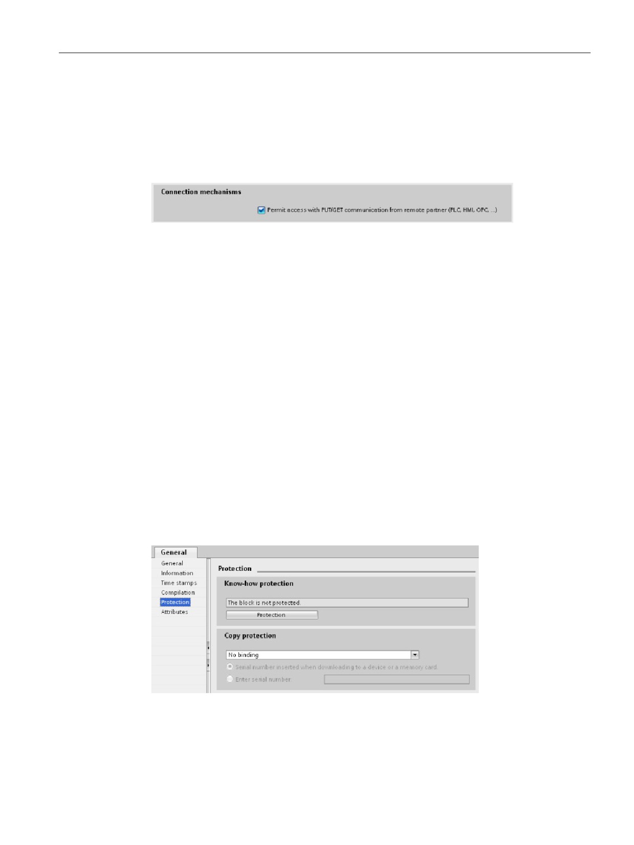
Connection mechanisms
To access remote connection partners with PUT/GET instructions, the user must also have
permission.
By default, the "Permit access with PUT/GET communication" option is not enabled. In this
case, read and write access to CPU data is only possible for communication connections
that require configuration or programming both for the local CPU and for the communication
partner. Access through BSEND/BRCV instructions is possible, for example.
Connections for which the local CPU is only a server (meaning that no
configuration/programming of the communication with the communication partner exists at
the local CPU), are therefore not possible during operation of the CPU, for example:
● PUT/GET, FETCH/WRITE or FTP access through communication modules
● PUT/GET access from other S7 CPUs
● HMI access through PUT/GET communication
88
Easy to create the device configuration
5.8 Protecting access to the CPU or code block is easy
If you want to allow access to CPU data from the client side, that is, you do not want to
restrict the communication services of the CPU, follow these steps:
1. Configure the protection access level to be any level other than "No access (complete
protection)".
2. Select the "Permit access with PUT/GET communication" check box.
When you download this configuration to the CPU, the CPU permits PUT/GET
communication from remote partners
5.8.1
Know-how protection
Know-how protection allows you to prevent one or more code blocks (OB, FB, FC, or DB) in
your program from unauthorized access. You create a password to limit access to the code
block. The password-protection prevents unauthorized reading or modification of the code
block. Without the password, you can read only the following information about the code
block:
● Block title, block comment, and block properties
● Transfer parameters (IN, OUT, IN_OUT, Return)
● Call structure of the program
● Global tags in the cross references (without information on the point of use), but local
tags are hidden
When you configure a block for "know-how" protection, the code within the block cannot be
accessed except after entering the password.
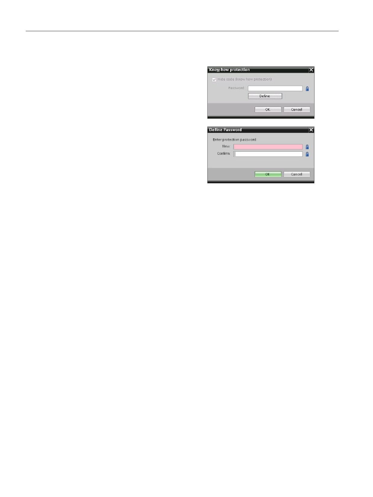
Use the "Properties" task card of the code block to configure the know-how protection for
that block. After opening the code block, select "Protection" from Properties.
89
Easy to create the device configuration
5.8 Protecting access to the CPU or code block is easy
1. In the Properties for the code block, click
the "Protection" button to display the
"Know-how protection" dialog.
2. Click the "Define" button to enter the
password.
After entering and confirming the password,
click "OK".
5.8.2
Copy protection
An additional security feature allows you to bind program blocks for use with a specific
memory card or CPU. This feature is especially useful for protecting your intellectual
property. When you bind a program block to a specific device, you restrict the program or
code block for use only with a specific memory card or CPU. This feature allows you to
distribute a program or code block electronically (such as over the Internet or through email)
or by sending a memory cartridge. Copy protection is available for OBs (Page 95), FBs
(Page 97), and FCs (Page 97). The S7-1200 CPU supports three types of block protection:
● Binding to the serial number of a CPU
● Binding to the serial number of a memory card
● Dynamic binding with mandatory password
90
Easy to create the device configuration
5.8 Protecting access to the CPU or code block is easy
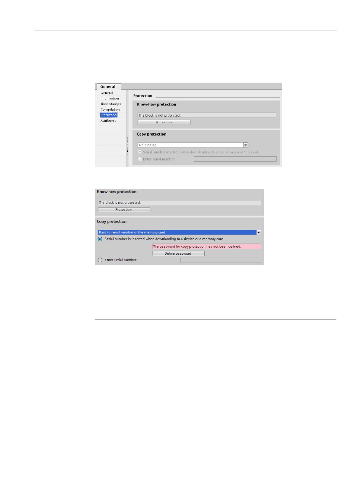
Use the "Properties" task card of the code block to bind the block to a specific CPU or
memory card.
1. After opening the code block, select "Protection".
2. From the drop-down list under "Copy protection" task, select the type of copy protection
that you want to use.
3. For binding to the serial number of a CPU or memory card, select either to insert the
serial number when downloading, or enter the serial number for the memory card or
CPU.
Note
The serial number is case-sensitive.
For dynamic binding with mandatory password, define the password that you must use to
download or copy the block.
When you subsequently download a block with dynamic binding, you must enter the
password to be able to download the block. Note that the copy protection password and
the know-how protection (Page 89) password are two separate passwords.
91
Easy to create the device configuration
5.8 Protecting access to the CPU or code block is easy
92
Programming made easy
6
6.1
Easy to design your user program
When you create a user program for the automation tasks, you insert the instructions for the
program into code blocks (OB, FB, or FC).
Choosing the type of structure for your user program
Based on the requirements of your application, you can choose either a linear structure or a
modular structure for creating your user program.
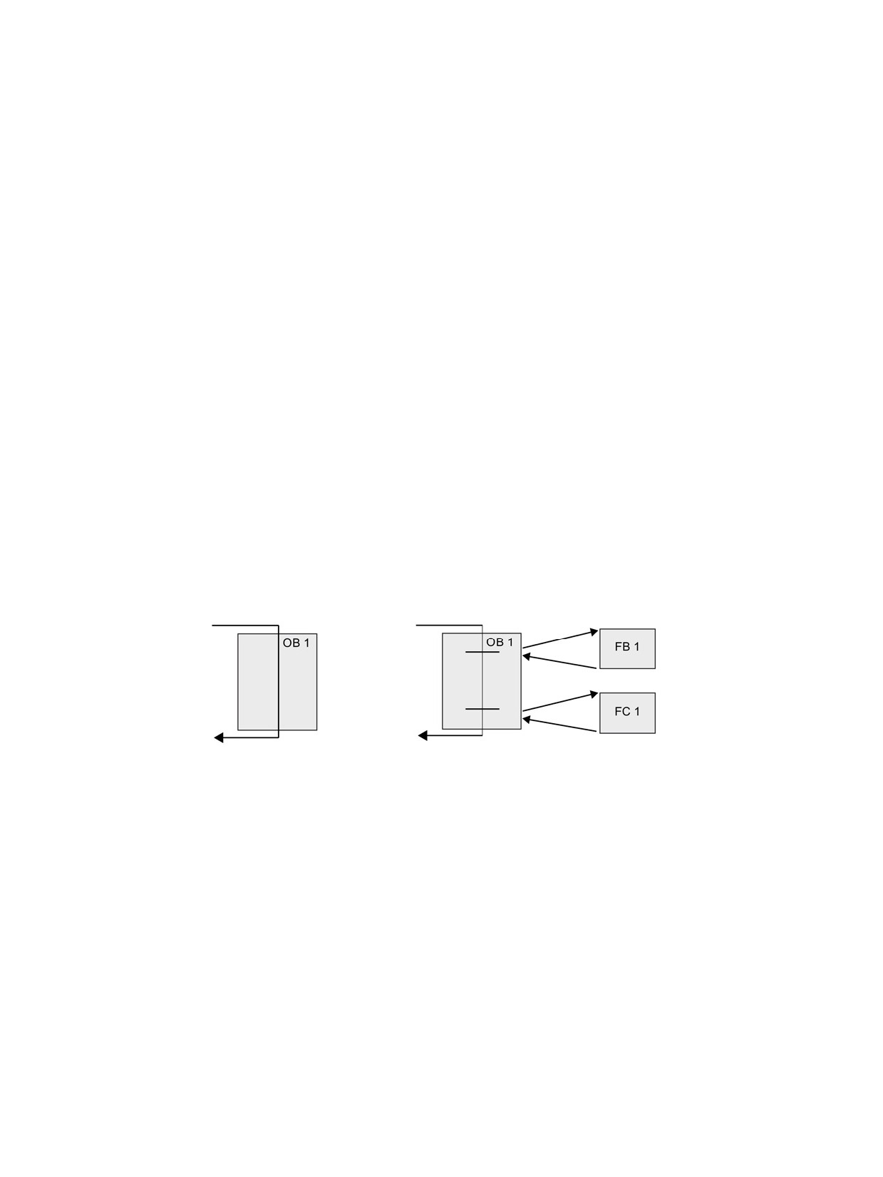
● A linear program executes all of the instructions for your automation tasks in sequence,
one after the other. Typically, the linear program puts all of the program instructions into
one program cycle OB (such as OB 1) for cyclic execution of the program.
● A modular program calls specific code blocks that perform specific tasks. To create a
modular structure, you divide the complex automation task into smaller subordinate tasks
that correspond to the functional tasks being performed by the process. Each code block
provides the program segment for each subordinate task. You structure your program by
calling one of the code blocks from another block.
Linear structure:
Modular structure:
By designing FBs and FCs to perform generic tasks, you create modular code blocks. You
then structure your user program by having other code blocks call these reusable modules.
The calling block passes device-specific parameters to the called block. When a code block
calls another code block, the CPU executes the program code in the called block. After
execution of the called block is complete, the CPU resumes the execution of the calling
block. Processing continues with execution of the instruction that follows after the block call.
93
Programming made easy
6.1 Easy to design your user program
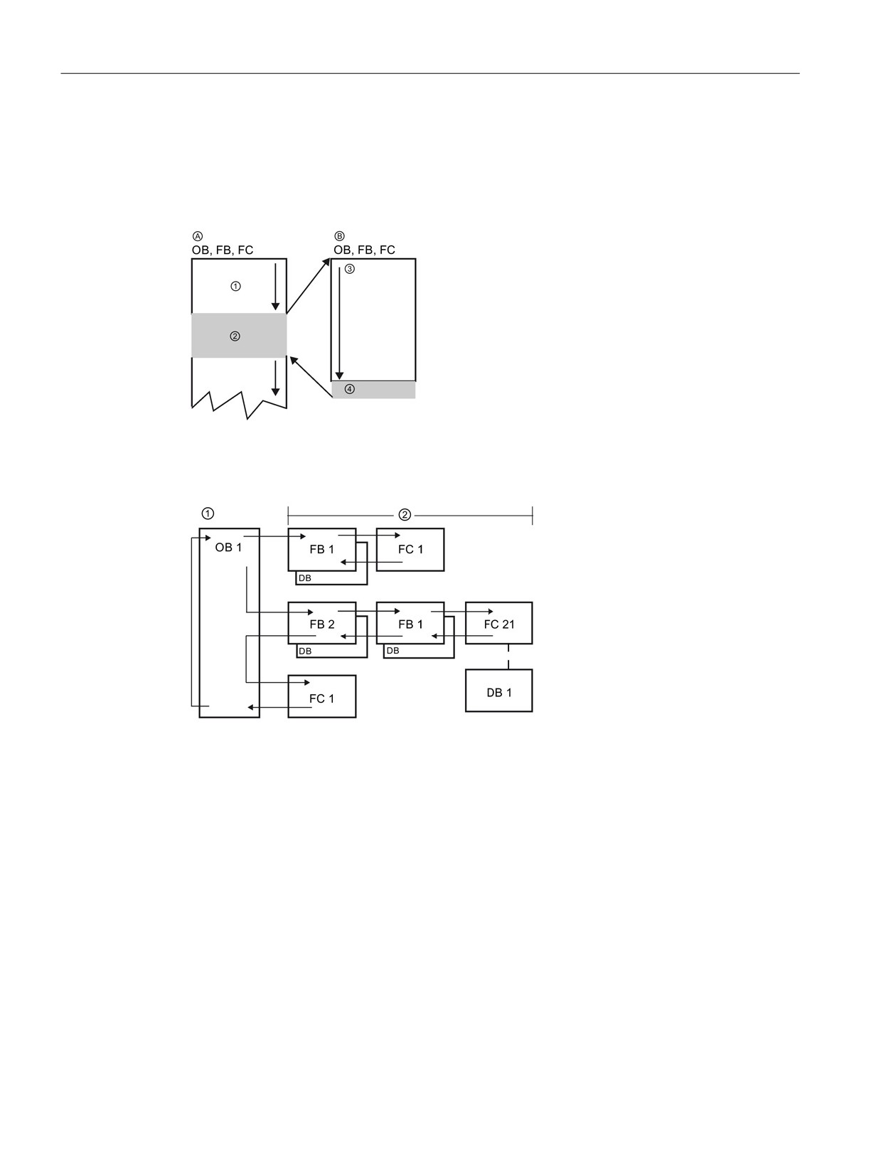
You can also assign an OB to an interrupting event. When the event occurs, the CPU
executes the program code in the associated OB. After the execution of the OB is complete,
the CPU resumes the execution at the point in the user program when the interrupting event
occurred, which could be any point in the scan.
A Calling block (or interrupted block)
B Called FB or BC (or interrupting OB)
① Program execution
② Instruction (or interrupting event) that initiates
the execution of another block
③ Program execution
④ Block end (returns to calling block)
You can nest the block calls for a more modular structure. In the following example, the
nesting depth is 3: the program cycle OB plus 3 layers of calls to code blocks.
① Start of cycle
② Nesting depth
By creating generic code blocks that can be reused within the user program, you can simplify
the design and implementation of the user program.
● You can create reusable blocks of code for standard tasks, such as for controlling a pump
or a motor. You can also store these generic code blocks in a library that can be used by
different applications or solutions.
● When you structure the user program into modular components that relate to functional
tasks, the design of your program can be easier to understand and to manage. The
modular components not only help to standardize the program design but can also help
to make updating or modifying the program code quicker and easier.
● Creating modular components simplifies the debugging of your program. By structuring
the complete program as a set of modular program segments, you can test the
functionality of each code block as it is developed.
● Utilizing a modular design that relates to specific functional tasks can reduce the time
required for the commissioning of the completed application.
94
Programming made easy
6.1 Easy to design your user program
6.1.1
Use OBs for organizing your user program
Organization blocks provide structure for your program. They serve as the interface between
the operating system and the user program. OBs are event driven. An event, such as a
diagnostic interrupt or a time interval, causes the CPU to execute an OB. Some OBs have
predefined start events and behavior.
The program cycle OB contains your main program. You can include more than one program
cycle OB in your user program. During RUN mode, the program cycle OBs execute at the
lowest priority level and can be interrupted by all other event types. The startup OB does not
interrupt the program cycle OB because the CPU executes the startup OB before going to
RUN mode.
After finishing the processing of the program cycle OBs, the CPU immediately executes the
program cycle OBs again. This cyclic processing is the "normal" type of processing used for
programmable logic controllers. For many applications, the entire user program is located in
a single program cycle OB.
You can create other OBs to perform specific functions, such as for handling interrupts and
errors, or for executing specific program code at specific time intervals. These OBs interrupt
the execution of the program cycle OBs.
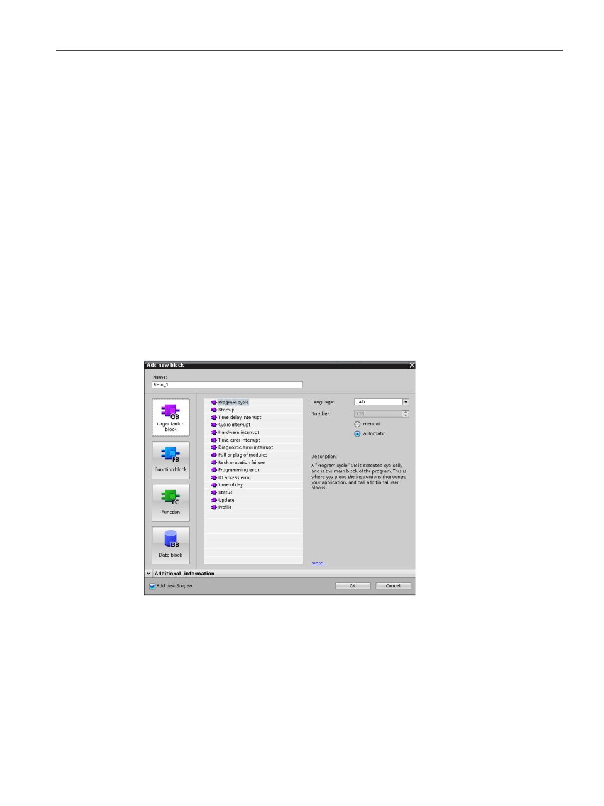
Use the "Add new block" dialog to create new OBs in your user program.
Interrupt handling is always
event-driven. When such
an event occurs, the CPU
interrupts the execution of
the user program and calls
the OB that was configured
to handle that event. After
finishing the execution of
the interrupting OB, the
CPU resumes the execu-
tion of the user program at
the point of interruption.
The CPU determines the order for handling interrupt events by priority. You can assign
multiple interrupt events to the same priority class. For more information, refer to the topics
on organization blocks (Page 57) and execution of the user program (Page 56).
95
Programming made easy
6.1 Easy to design your user program
Creating additional OBs
You can create multiple OBs for your user program, even for the program cycle and startup
OB events. Use the "Add new block" dialog to create an OB and enter a name for your OB.
If you create multiple program cycle OBs for your user program, the CPU executes each
program cycle OB in numerical sequence, starting with the program cycle OB with the lowest
number (such as OB 1). For example: after the first program cycle OB (such as OB 1)
finishes, the CPU executes the program cycle OB with the next higher number.
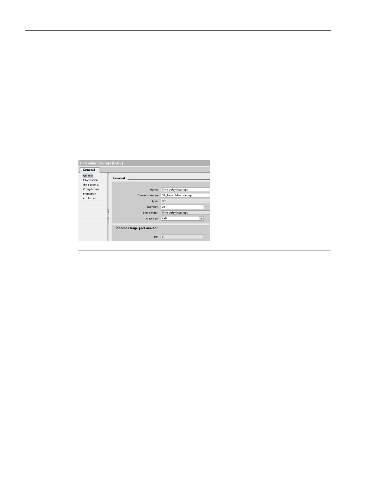
Configuring the properties of an OB
You can modify the properties of an OB. For example, you can configure the OB number or
programming language.
Note
Note that you can assign a process image part number to an OB that corresponds to PIP0,
PIP1, PIP2, PIP3, or PIP4. If you enter a number for the process image part number, the
CPU creates that process image partition. See the topic "Execution of the user program
(Page 56)" for an explanation of the process image partitions.
96
Programming made easy
6.1 Easy to design your user program
6.1.2
FBs and FCs make programming the modular tasks easy
A function (FC) is like a subroutine. An FC is a code block that typically performs a specific
operation on a set of input values. The FC stores the results of this operation in memory
locations. Use FCs to perform the following tasks:
● To perform standard and reusable operations, such as for mathematical calculations
● To perform functional tasks, such as for individual controls using bit logic operations
An FC can also be called several times at different points in a program. This reuse simplifies
the programming of frequently recurring tasks.
Unlike an FB, an FC does not have an associated instance DB. The FC uses its temp
memory (L) for the data used to calculate the operation. The temporary data is not saved. To
store data for use after the execution of the FC has finished, assign the output value to a
global memory location, such as M memory or to a global DB.
A function block (FB) is like a subroutine with memory. An FB is a code block whose calls
can be programmed with block parameters. The FB stores the input (IN), output (OUT), and
in/out (IN_OUT) parameters in variable memory that is located in a data block (DB), or
"instance" DB. The instance DB provides a block of memory that is associated with that
instance (or call) of the FB and stores data after the FB finishes.
You typically use an FB to control the operation for tasks or devices that do not finish their
operation within one scan cycle. To store the operating parameters so that they can be
quickly accessed from one scan to the next, each FB in your user program has one or more
instance DBs. When you call an FB, you also open an instance DB that stores the values of
the block parameters and the static local data for that call or "instance" of the FB. These
values are stored in the instance DB after the FB finishes.
You can assign start values to the parameters in the FB interface. These values are
transferred to the associated instance DB. If you do not assign parameters, the values
currently stored in the instance DB will be used. In some cases, you must assign
parameters.
You can associate different instance DBs with different calls of the FB. The instance DBs
allow you to use one generic FB to control multiple devices. You structure your program by
having one code block make a call to an FB and an instance DB. The CPU then executes
the program code in that FB and stores the block parameters and the static local data in the
instance DB. When the execution of the FB finishes, the CPU returns to the code block that
called the FB. The instance DB retains the values for that instance of the FB. By designing
the FB for generic control tasks, you can reuse the FB for multiple devices by selecting
different instance DBs for different calls of the FB.
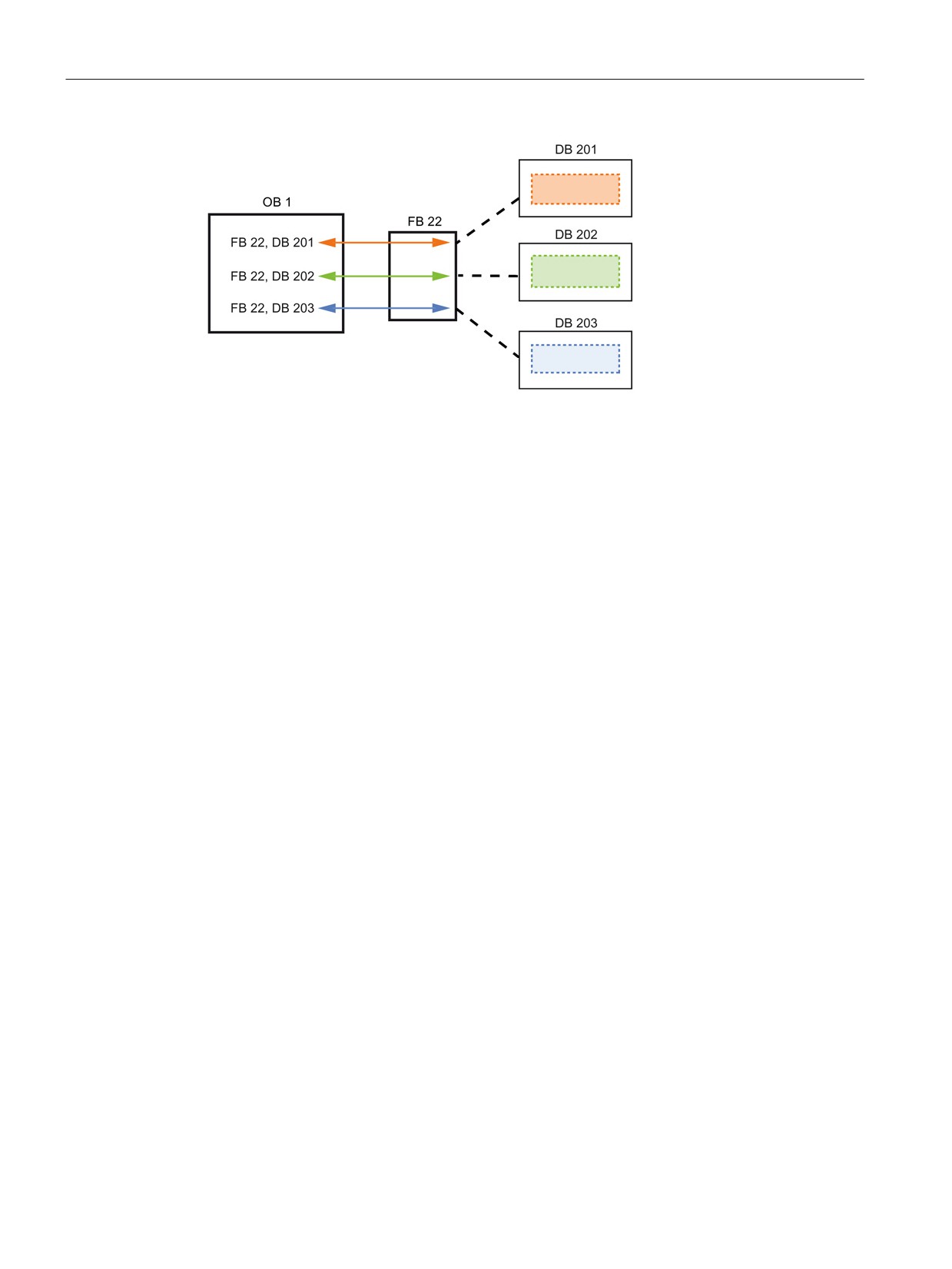
The following figure shows an OB that calls one FB three times, using a different data block
for each call. This structure allows one generic FB to control several similar devices, such as
motors, by assigning a different instance data block for each call for the different devices.
97
Programming made easy
6.1 Easy to design your user program
Each instance DB stores the data (such as speed, ramp-up time, and total operating time)
for an individual device. In this example, FB 22 controls three separate devices, with DB 201
storing the operational data for the first device, DB 202 storing the operational data for the
second device, and DB 203 storing the operational data for the third device.
6.1.3
Data blocks provide easy storage for program data
You create data blocks (DB) in your user program to store data for the code blocks. All of the
program blocks in the user program can access the data in a global DB, but an instance DB
stores data for a specific function block (FB).
Your user program can store data in the specialized memory areas of the CPU, such as for
the inputs (I), outputs (Q), and bit memory (M). In addition, you can use a data block (DB) for
fast access to data stored within the program itself.
The data stored in a DB is not deleted when the data block is closed or the execution of the
associated code block comes to an end. There are two types of DBs:
● A global DB stores data for the code blocks in your program. Any OB, FB, or FC can
access the data in a global DB.
● An instance DB stores the data for a specific FB. The structure of the data in an instance
DB reflects the parameters (Input, Output, and InOut) and the static data for the FB. The
Temp memory for the FB is not stored in the instance DB.
Although the instance DB reflects the data for a specific FB, any code block can access the
data in an instance DB.
98
Programming made easy
6.1 Easy to design your user program
6.1.4
Creating a new code block
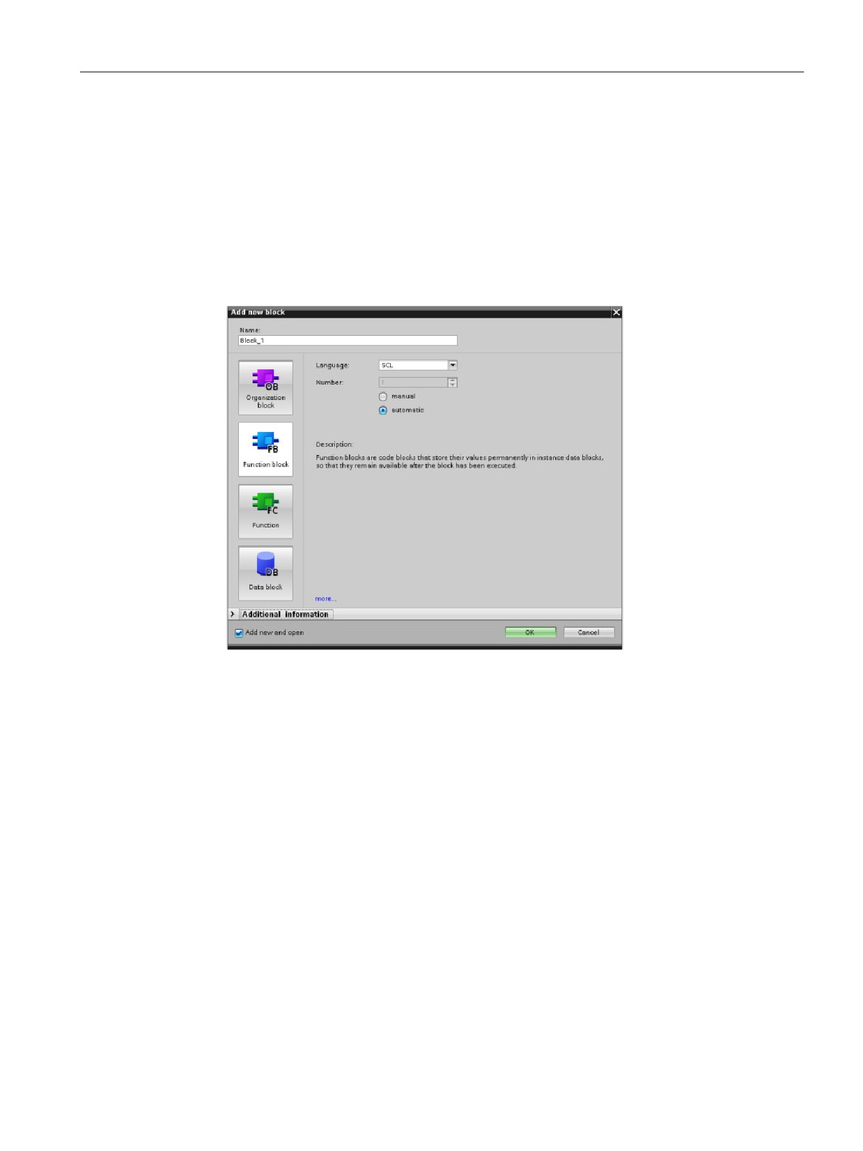
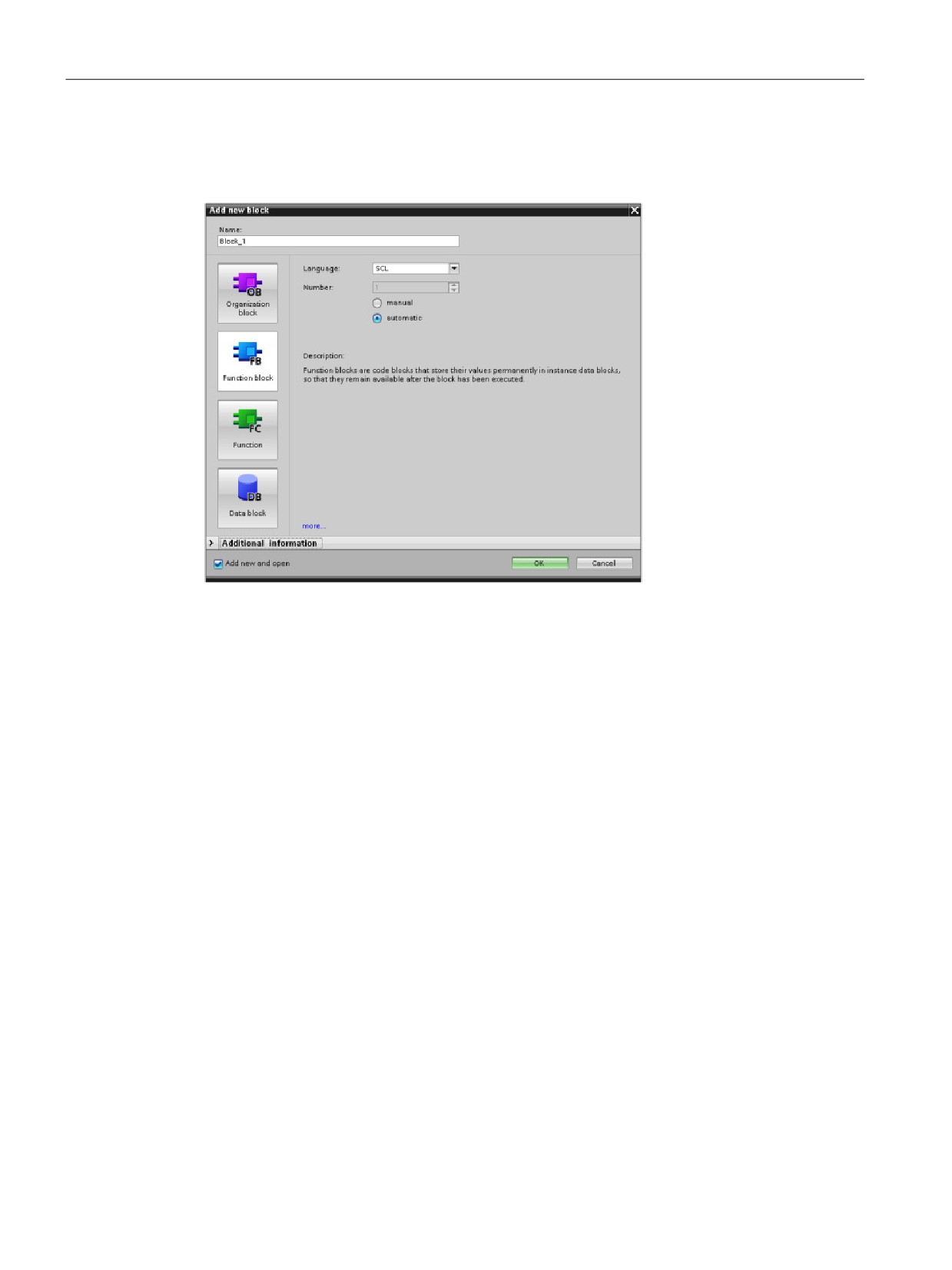
To add a new code block to the program, follow these steps:
1. Open the "Program blocks" folder.
2. Double-click "Add new block".
3. In the "Add new block" dialog, click the type of block to add. For example, click the
"Function (FC)" icon to add an FC.
4. Select the programming language for the code block from the drop-down menu.
5. Click "OK" to add the block to the project.
Selecting the "Add new and open" option (default) causes STEP 7 to open the newly-created
block in the editor.
99
Programming made easy
6.1 Easy to design your user program
6.1.5
Creating reusable code blocks
Use the "Add new block"
dialog under "Program
blocks" in the Project navi-
gator to create OBs, FBs,
FCs, and global DBs.
When you create a code
block, you select the pro-
gramming language for the
block. You do not select a
language for a DB because
it only stores data.
Selecting the "Add new
and open" check box (de-
fault) opens the code block
in the Project view.
You can store objects you want to reuse in libraries. For each project, there is a project
library that is connected to the project. In addition to the project library, you can create any
number of global libraries that can be used over several projects. Since the libraries are
compatible with each other, library elements can be copied and moved from one library to
another.
Libraries are used, for example, to create templates for blocks that you first paste into the
project library and then further develop there. Finally, you copy the blocks from the project
library to a global library. You make the global library available to other colleagues working
on your project. They use the blocks and further adapt them to their individual requirements,
where necessary.
For details about library operations, refer to the STEP 7 online Help library topics.
100

Programming made easy
6.2 Easy-to-use programming languages
6.1.6
Calling a code block from another code block
You can easily have any code block (OB,
FB, or FC) in your user program call an FB
or FC in your CPU.
1. Open the code block that will call the other block.
2. In the project tree, select the code block to be called.
3. Drag the block to the selected network to create a call to the code block.
Note
Your user program cannot call an OB because OBs are event-driven (Page 58). The CPU
starts the execution of the OB in response to receiving an event.
6.2
Easy-to-use programming languages
STEP 7 provides the following standard programming languages for S7-1200:
● LAD (ladder logic) is a graphical programming language. The representation is based on
circuit diagrams (Page 102).
● FBD (Function Block Diagram) is a programming language that is based on the graphical
logic symbols used in Boolean algebra (Page 103).
● SCL (structured control language) is a text-based, high-level programming language
(Page 103).
When you create a code block, you select the programming language to be used by that
block.
Your user program can utilize code blocks created in any or all of the programming
languages.
101
Programming made easy
6.2 Easy-to-use programming languages
6.2.1
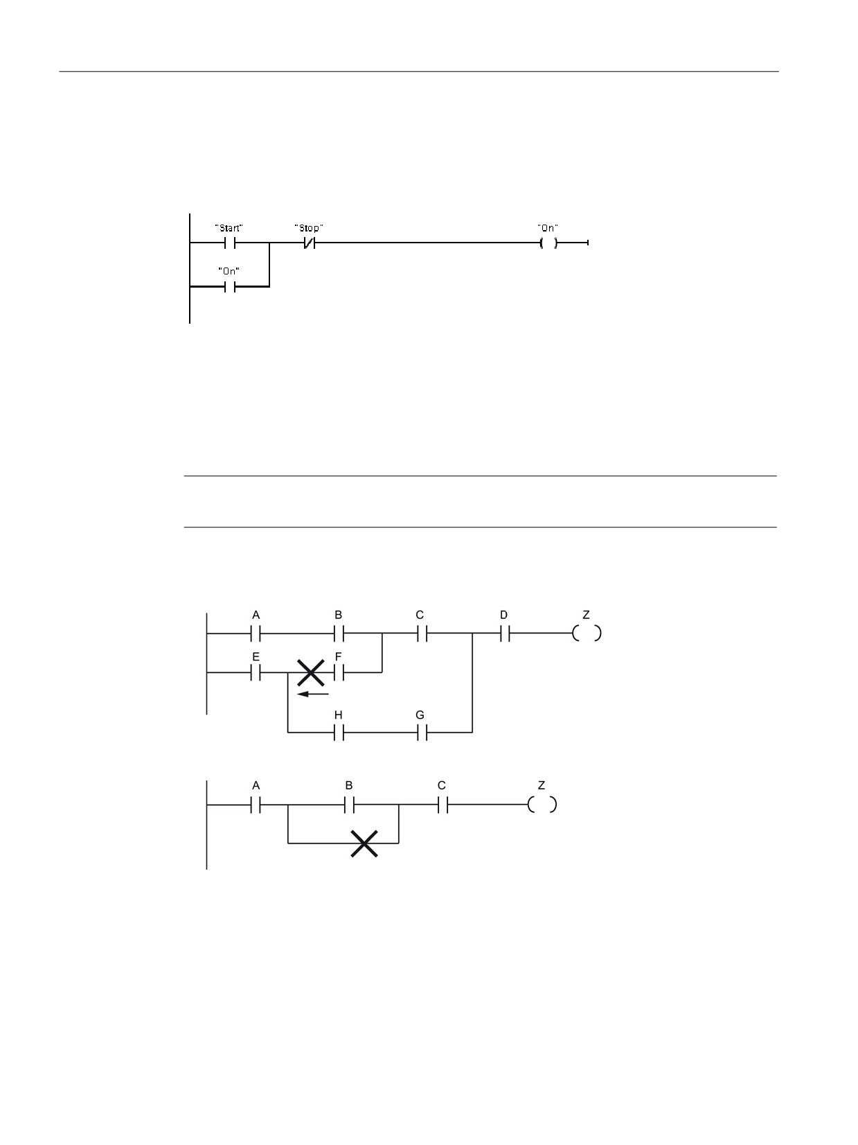
Ladder logic (LAD)
The elements of a circuit diagram, such as normally closed and normally open contacts, and
coils are linked to form networks.
To create the logic for complex operations, you can insert branches to create the logic for
parallel circuits. Parallel branches are opened downwards or are connected directly to the
power rail. You terminate the branches upwards.
LAD provides "box" instructions for a variety of functions, such as math, timer, counter, and
move.
STEP 7 does not limit the number of instructions (rows and columns) in a LAD network.
Note
Every LAD network must terminate with a coil or a box instruction.
Consider the following rules when creating a LAD network:
● You cannot create a branch that could result in a power flow in the reverse direction.
● You cannot create a branch that would cause a short circuit.
102
Programming made easy
6.2 Easy-to-use programming languages
6.2.2
Function Block Diagram (FBD)
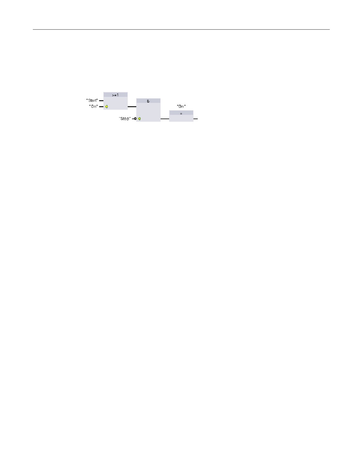
Like LAD, FBD is also a graphical programming language. The representation of the logic is
based on the graphical logic symbols used in Boolean algebra.
To create the logic for complex operations,
insert parallel branches between the boxes.
Mathematical functions and other complex functions can be represented directly in
conjunction with the logic boxes.
STEP 7 does not limit the number of instructions (rows and columns) in an FBD network.
6.2.3
SCL overview
Structured Control Language (SCL) is a high-level, PASCAL-based programming language
for the SIMATIC S7 CPUs. SCL supports the block structure of STEP 7. You can also
include program blocks written in SCL with program blocks written in LAD and FBD.
SCL instructions use standard programming operators, such as for assignment (:=),
mathematical functions (+ for addition, - for subtraction, * for multiplication, and / for division).
SCL uses standard PASCAL program control operations, such as IF-THEN-ELSE, CASE,
REPEAT-UNTIL, GOTO and RETURN. You can use any PASCAL reference for syntactical
elements of the SCL programming language. Many of the other instructions for SCL, such as
timers and counters, match the LAD and FBD instructions.
Because SCL, like PASCAL, offers conditional processing, looping, and nesting control
structures, you can implement complex algorithms in SCL more easily than in LAD or FBD.
The following examples show different expressions for different uses:
"C" := #A+#B;
Assigns two local variables to a tag
"Data_block_1".Tag := #A;
Assignment to a data block tag
IF #A > #B THEN "C" := #A;
Condition for the IF-THEN statement
"C" := SQRT (SQR (#A) + SQR (#B));
Parameters for the SQRT instruction
As a high-level programming language, SCL uses standard statements for basic tasks:
● Assignment statement: :=
● Mathematical functions: +, -, *, and /
● Addressing of global variables (tags): "<tag name>" (Tag name or data block name
enclosed in double quotes)
● Addressing of local variables: #<variable name> (Variable name preceded by "#" symbol)
● Absolute addressing: %<absolute address>, for example %I0.0 or %MW10
Arithmetic operators can process various numeric data types. The data type of the result is
determined by the data type of the most-significant operands. For example, a multiplication
operation that uses an INT operand and a REAL operand yields a REAL value for the result.
103
Programming made easy
6.2 Easy-to-use programming languages
6.2.4
SCL program editor
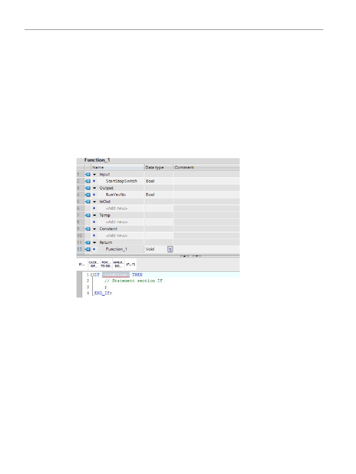
You can designate any type of block (OB, FB, or FC) to use the SCL programming language
at the time you create the block. STEP 7 provides an SCL program editor that includes the
following elements:
● Interface section for defining the parameters of the code block
● Code section for the program code
● Instruction tree that contains the SCL instructions supported by the CPU
You enter the SCL code for your instruction directly in the code section. The editor includes
buttons for common code constructs and comments. For more complex instructions, simply
drag the SCL instructions from the instruction tree and drop them into your program. You can
also use any text editor to create an SCL program and then import that file into STEP 7.
In the Interface section of the SCL code block you can declare the following types of
parameters:
● Input, Output, InOut, and Ret_Val: These parameters define the input tags, output tags,
and return value for the code block. The tag name that you enter here is used locally
during the execution of the code block. You typically would not use the global tag name in
the tag table.
● Static (FBs only; the illustration above is for an FC): The code block uses static tags for
storage of static intermediate results in the instance data block. The block retains static
data until overwritten, which can be after several cycles. The names of the blocks, which
this block calls as multi-instance, are also stored in the static local data.
● Temp: These parameters are the temporary tags that are used during the execution of
the code block.
● Constant: These are named constant values for your code block.
104
Programming made easy
6.3 Powerful instructions make programming easy
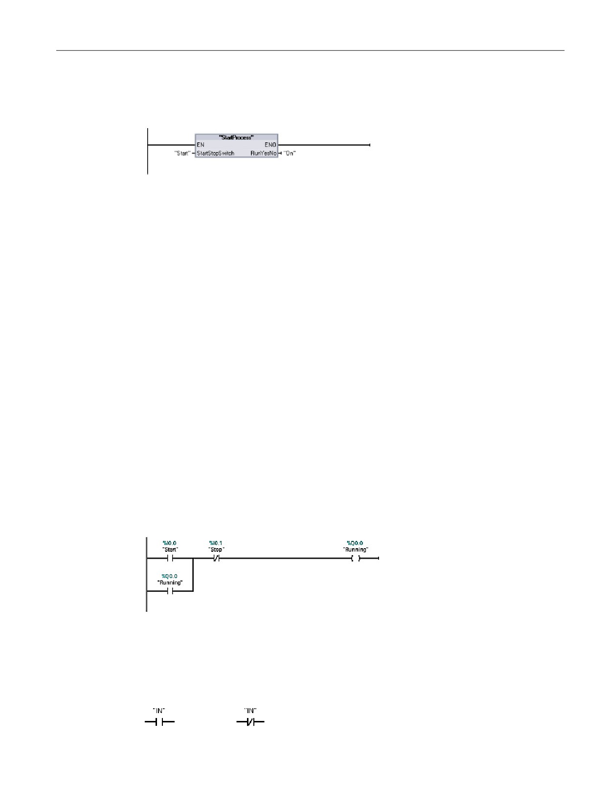
If you call the SCL code block from another code block, the parameters of the SCL code
block appear as inputs or outputs.
In this example, the tags for "Start" and "On" (from the project tag table) correspond to
"StartStopSwitch" and "RunYesNo" in the declaration table of the SCL program.
6.3
Powerful instructions make programming easy
6.3.1
Providing the basic instructions you expect
The S7-1200 CPU supports many instructions. They are available from the instruction tree in
STEP 7 in the following groups:
● Basic instructions
● Extended instructions
● Technology
● Communication instruction
You can find a complete summary of all the instructions in the S7-1200 Programmable
Controller System Manual. This manual describes many of the common instructions.
Bit logic instructions
The basis of bit logic instructions is contacts and coils. Contacts read the status of a bit,
while the coils write the status of the operation to a bit.
Contacts test the binary status of
the bit, with the result being "power
flow" if on (1) or "no power flow" if
off (0).
The state of the coil reflects the
status of the preceding logic.
If you use a coil with the same address in more than one program location, the result of the
last calculation in the user program determines the status of the value that is written to the
physical output during the updating of the outputs.
Normally Open
Normally Closed
The Normally Open contact is closed (ON) when
Contact
Contact
the assigned bit value is equal to 1.
The Normally Closed contact is closed (ON) when
the assigned bit value is equal to 0.
105

Programming made easy
6.3 Powerful instructions make programming easy
The basic structure of a bit logic operation is either AND logic or OR logic. Contacts
connected in series create AND logic networks. Contacts connected in parallel create OR
logic networks.
You can connect contacts to other contacts and create your own combination logic. If the
input bit you specify uses memory identifier I (input) or Q (output), then the bit value is read
from the process-image register. The physical contact signals in your control process are
wired to input terminals on the PLC. The CPU scans the wired input signals and updates the
corresponding state values in the process-image input register.
You can specify an immediate read of a physical input using ":P" following the tag for an
input (such as "Motor_Start:P" or "I3.4:P"). For an immediate read, the bit data values are
read directly from the physical input instead of the process image. An immediate read does
not update the process image.
Output coil
Inverted output coil
Note the following output results for power flow through output and inverted output coils:
● If there is power flow through an output coil, then the output bit is set to 1.
● If there is no power flow through an output coil, then the output coil bit is set to 0.
● If there is power flow through an inverted output coil, then the output bit is set to 0.
● If there is no power flow through an inverted output coil, then the output bit is set to 1.
The coil output instruction writes a value for an output bit. If the output bit you specify uses
memory identifier Q, then the CPU turns the output bit in the process-image register on or
off, setting the specified bit equal to power flow status. The output signals for your control
actuators are wired to the output terminals on the PLC. In RUN mode, the CPU system
scans your input signals, processes the input states according to your program logic, and
then reacts by setting new output state values in the process-image output register. After
each program execution cycle, the CPU transfers the new output state reaction stored in the
process-image register to the wired output terminals.
You can specify an immediate write of a physical output using ":P" following the tag for an
output (such as "Motor_On:P" or "Q3.4:P"). For an immediate write, the bit data values are
written to the process image output and directly to the physical output.
Coils are not restricted to the end of a network. You can insert a coil in the middle of a rung
of the LAD network, in between contacts or other instructions.
NOT contact inverter
AND box with one inverted
AND box with inverted logic input and
(LAD)
logic input (FBD)
output (FBD)
The LAD NOT contact inverts the logical state of power flow input.
● If there is no power flow into the NOT contact, then there is power flow out.
● If there is power flow into the NOT contact, then there is no power flow out.
106

Programming made easy
6.3 Powerful instructions make programming easy
For FBD programming, you can drag the "Invert RLO" tool from the "Favorites" toolbar or
instruction tree and then drop it on an input or output to create a logic inverter on that box
connector.
AND box (FBD)
OR box (FBD)
XOR box (FBD)
● All inputs of an AND box must be TRUE for the output to be TRUE.
● Any input of an OR box must be TRUE for the output to be TRUE.
● An odd number of the inputs of an XOR box must be TRUE for the output to be TRUE.
In FBD programming, the contact networks of LAD are represented by AND (&), OR (>=1),
and EXCLUSIVE OR (x) box networks where you can specify bit values for the box inputs
and outputs. You may also connect to other logic boxes and create your own logic
combinations. After the box is placed in your network, you can drag the "Insert input" tool
from the "Favorites" toolbar or instruction tree and then drop it onto the input side of the box
to add more inputs. You can also right-click on the box input connector and select "Insert
input".
Box inputs and output can be connected to another logic box, or you can enter a bit address
or bit symbol name for an unconnected input. When the box instruction is executed, the
current input states are applied to the binary box logic and, if true, the box output will be true.
107
Programming made easy
6.3 Powerful instructions make programming easy
6.3.2
Comparator and Move instructions
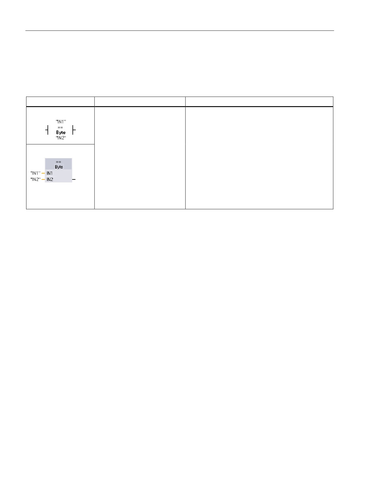
The Comparator operations perform a comparison of two values with the same data type.
Table 6- 1
Comparator operations
Instruction
SCL
Description
LAD:
out := in1 = in2;
• Equal (==):The comparison is true if IN1 is equal to
out := in1 <> in2;
IN2
out := in1 >= in2;
• Not equal (<>):The comparison is true if IN1 is not
out := in1 <= in2;
equal to IN2
out := in1 > in2;
• Greater or equal (>=):The comparison is true if IN1 is
FBD:
out := in1 < in2;
greater than or equal to IN2
• Less or equal (<=):The comparison is true if IN1 is
less than or equal to IN2
• Greater than (>):The comparison is true if IN1 is
greater than IN2
• Less than (<):The comparison is true if IN1 is less
than IN2
1
For LAD and FBD: The contact is activated (LAD) or the box output is TRUE (FBD) if the comparison is TRUE,
For additional Comparator operations, refer to the S7-1200 Programmable Controller System
Manual.
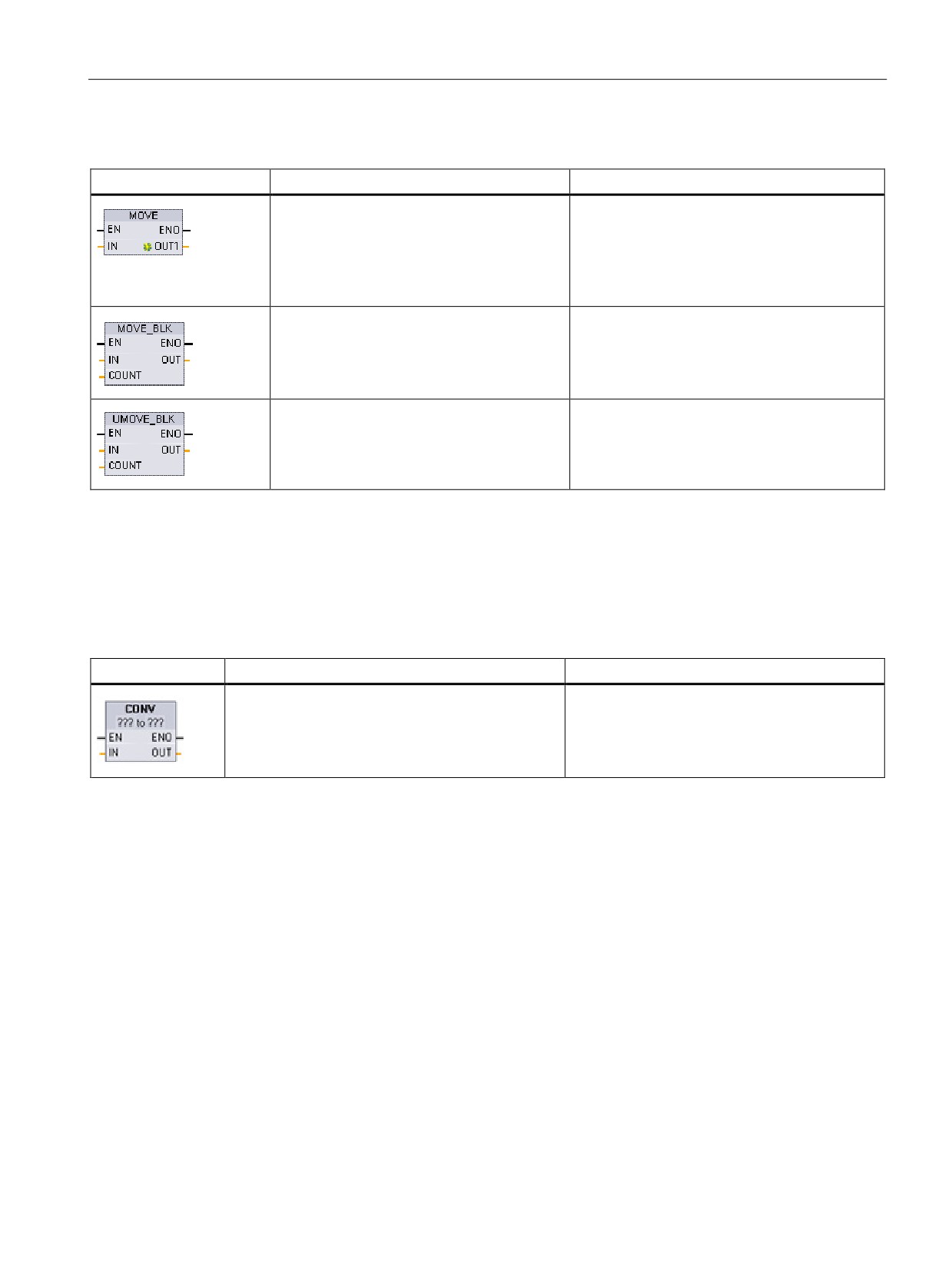
The Move operations copy data elements to a new memory address and can convert from
one data type to another. The source data is not changed by the move process.
● MOVE copies a data element stored at a specified address to a new address. To add
another output, click the icon next to the OUT1 parameter.
● MOVE_BLK (interruptible move) and UMOVE_BLK (uninterruptible move) copy a block of
data elements to a new address. The MOVE_BLK and UMOVE_BLK instructions have an
additional COUNT parameter. The COUNT specifies how many data elements are
copied. The number of bytes per element copied depends on the data type assigned to
the IN and OUT parameter tag names in the PLC tag table.
108
Programming made easy
6.3 Powerful instructions make programming easy
Table 6- 2
MOVE, MOVE_BLK and UMOVE_BLK instructions
LAD / FBD
SCL
Description
out1 := in;
Copies a data element stored at a specified
address to a new address or multiple address-
es. To add another output in LAD or FBD, click
the icon by the output parameter. For SCL, use
multiple assignment statements. You might
also use one of the loop constructions.
MOVE_BLK(in:=_variant_in,
Interruptible move that copies a block of data
count:=_uint_in,
elements to a new address.
out=>_variant_out);
UMOVE_BLK(in:=_variant_in,
Uninterruptible move that copies a block of
count:=_uint_in
data elements to a new address.
out=>_variant_out);
For additional Move operations, refer to the S7-1200 System Manual.
6.3.3
Conversion operations
Table 6- 3
Conversion operations
LAD / FBD
SCL
Description
out := <data type in>_TO_<data type
Converts a data element from one data type to
out>(in);
another data type.
1
For LAD and FBD: Click below the box name and select the data types from the drop-down menu. After you select the
(convert from) data type, a list of possible conversions is shown in the (convert to) dropdown list.
2
For SCL: Construct the conversion instruction by identifying the data type for the input parameter (in) and output pa-
rameter (out). For example, DWORD_TO_REAL converts a DWord value to a Real value.
109
Programming made easy
6.3 Powerful instructions make programming easy
Table 6- 4
Round and Truncate instructions
LAD / FBD
SCL
Description
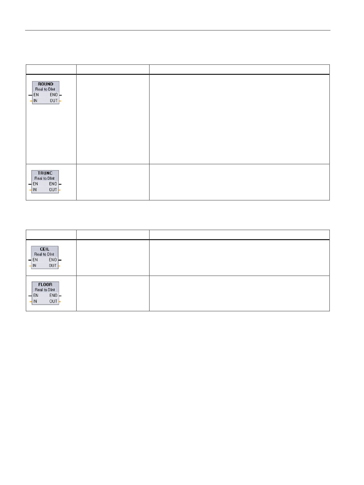
out := ROUND (in);
Converts a real number (Real or LReal) to an integer. The instruction
rounds the real number to the nearest integer value (IEEE - round to
nearest). If the number is exactly one-half the span between two inte-
gers (for example, 10.5), then the instruction rounds the number to the
even integer. For example:
• ROUND (10.5) = 10
• ROUND (11.5) = 12
For LAD/FBD, you click the "???" in the instruction box to select the
data type for the output, for example, "DInt". For SCL, the default output
data type is DINT. To round to another output data type, enter the in-
struction name with the explicit name of the data type, for example,
ROUND_REAL or ROUND_LREAL.
out := TRUNC(in);
Converts a real number (Real or LReal) to an integer. The fractional
part of the real number is truncated to zero (IEEE - round to zero).
Table 6- 5
Ceiling (CEIL) and Floor instructions
LAD / FBD
SCL
Description
out := CEIL(in);
Converts a real number (Real or LReal) to the closest integer greater
than or equal to the selected real number (IEEE "round to +infinity").
out := FLOOR(in);
Converts a real number (Real or LReal) to the closest integer smaller
than or equal to the selected real number (IEEE "round to -infinity").
110
Programming made easy
6.3 Powerful instructions make programming easy
Table 6- 6
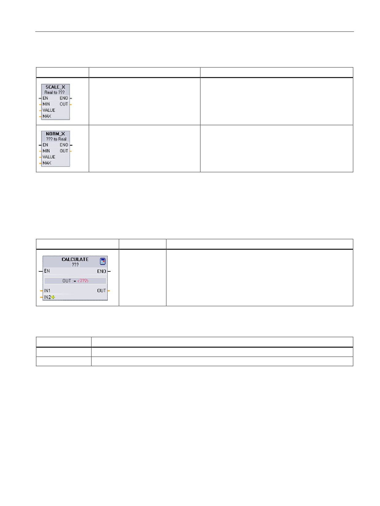
SCALE_X and NORM_X instructions
LAD / FBD
SCL
Description
out := SCALE_X(
Scales the normalized real parameter VALUE where ( 0.0
min:=_in_,
<= VALUE <= 1.0 ) in the data type and value range spec-
value:=_in_,
ified by the MIN and MAX parameters:
max:=_in_);
OUT = VALUE (MAX - MIN) + MIN
out := NORM_X(
Normalizes the parameter VALUE inside the value range
min:=_in_,
specified by the MIN and MAX parameters:
value:=_in_,
OUT = (VALUE - MIN) / (MAX - MIN),
max:=_in_);
where ( 0.0 <= OUT <= 1.0 )
1
Equivalent SCL: out := value (max-min) + min;2 Equivalent SCL: out := (value-min)/(max-min);
6.3.4
Math made easy with the Calculate instruction
Table 6- 7
CALCULATE instruction
LAD / FBD
SCL
Description
Use the stand-
The CALCULATE instruction lets you create a math function that oper-
ard SCL math
ates on inputs (IN1, IN2, .. INn) and produces the result at OUT, ac-
expressions to
cording to the equation that you define.
create the equa-
• Select a data type first. All inputs and the output must be the same
tion.
data type.
• To add another input, click the icon at the last input.
Table 6- 8
Data types for the parameters
Parameter
Data type1
IN1, IN2, ..INn
SInt, Int, DInt, USInt, UInt, UDInt, Real, LReal, Byte, Word, DWord
OUT
SInt, Int, DInt, USInt, UInt, UDInt, Real, LReal, Byte, Word, DWord
1
The IN and OUT parameters must be the same data type (with implicit conversions of the input parameters). For exam-
ple: A SINT value for an input would be converted to an INT or a REAL value if OUT is an INT or REAL
111
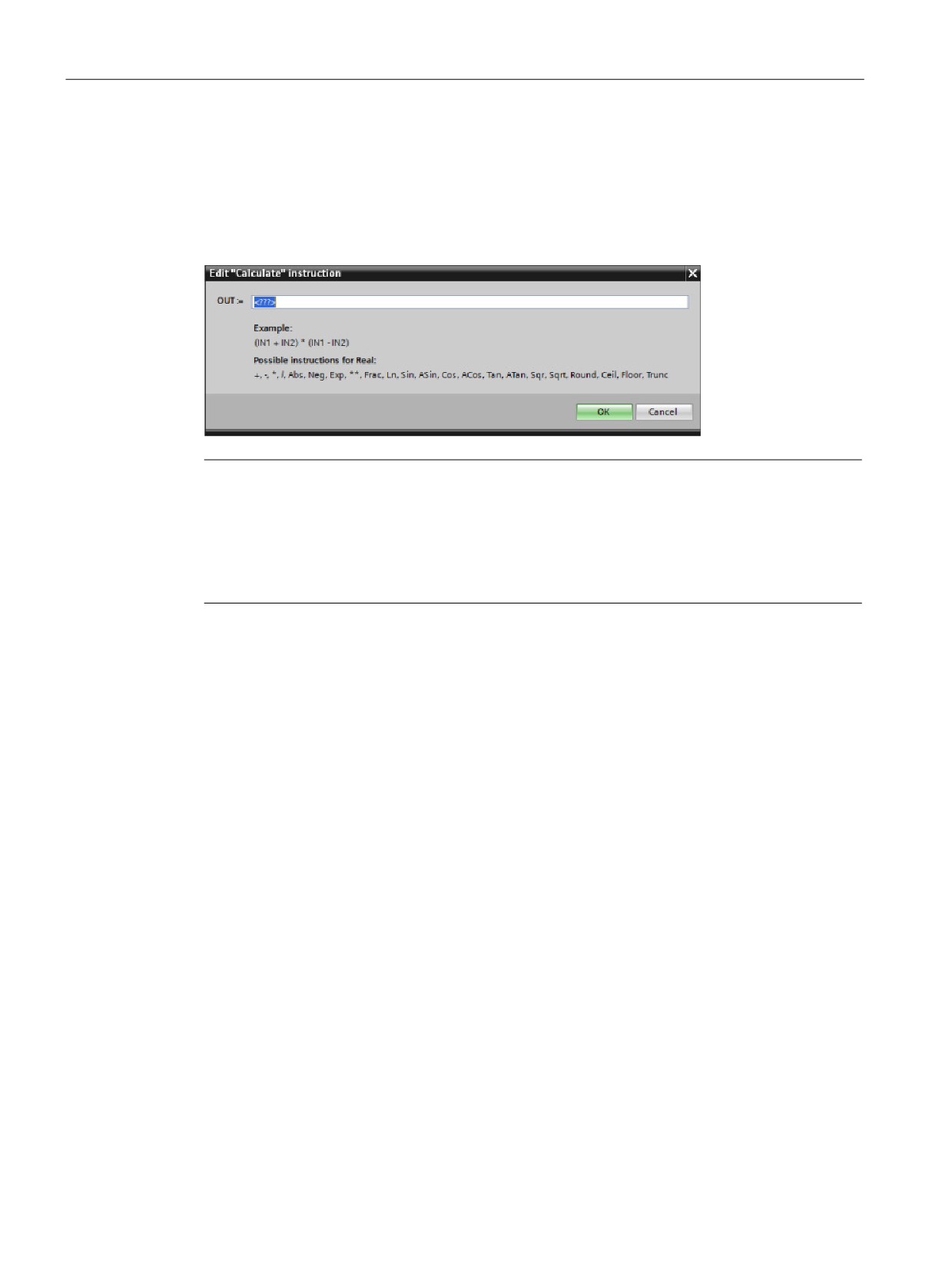
Programming made easy
6.3 Powerful instructions make programming easy
Click the calculator icon to open the dialog and define your math function. You enter your
equation as inputs (such as IN1 and IN2) and operations. When you click "OK" to save the
function, the dialog automatically creates the inputs for the CALCULATE instruction.
The dialog shows an example and a list of possible instructions that you can include based
on the data type of the OUT parameter:
Note
You also must create an input for any constants in your function. The constant value would
then be entered in the associated input for the CALCULATE instruction.
By entering constants as inputs, you can copy the CALCULATE instruction to other locations
in your user program without having to change the function. You then can change the values
or tags of the inputs for the instruction without modifying the function.
When CALCULATE is executed and all the individual operations in the calculation complete
successfully, then the ENO = 1. Otherwise, ENO = 0.
For an example of the CALCULATE instruction, see "Use the CALCULATE instruction for a
complex mathematical equation (Page 46)".
112
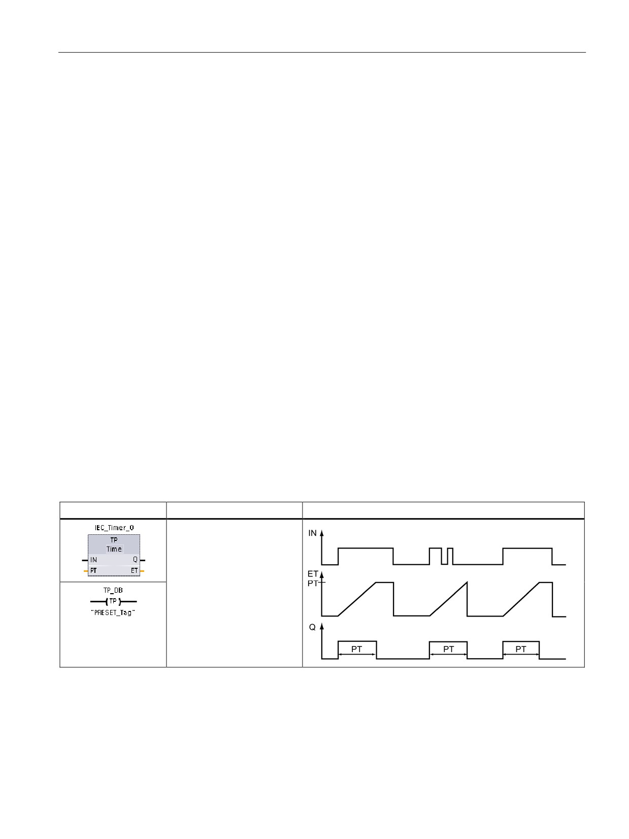
Programming made easy
6.3 Powerful instructions make programming easy
6.3.5
Timer operations
The S7-1200 supports the following timers
● The TP timer generates a pulse with a preset width time.
● The TON timer sets the output (Q) to ON after a preset time delay.
● The TOF timer sets the output (Q) to ON and then resets the output to OFF after a preset
time delay.
● The TONR timer sets the output (Q) to ON after a preset time delay. The elapsed time is
accumulated over multiple timing periods until the reset (R) input is used to reset the
elapsed time.
● The PT (preset timer) coil loads a new preset time value in the specified timer.
● The RT (reset timer) coil resets the specified timer.
For LAD and FBD, these instructions are available as either a box instruction or an output
coil.
The number of timers that you can use in your user program is limited only by the amount of
memory in the CPU. Each timer uses 16 bytes of memory.
Each timer uses a structure stored in a data block to maintain timer data. For SCL, you must
first create the DB for the individual timer instruction before you can reference it. For LAD
and FBD, STEP 7 automatically creates the DB when you insert the instruction.
When you create the DB, you can also use a multi-instance DB. Because the timer data is
contained in a single DB and does not require a separate DB for each timer, the processing
time for handling the timers is reduced. There is no interaction between the timer data
structures in the shared multi-instance DB.
Table 6- 9
TP (Pulse timer)
LAD / FBD
SCL
Timing diagram
"timer_db".TP(
IN:=_bool_in_,
PT:=_time_in_,
Q=>_bool_out_,
ET=>_time_out_);
113
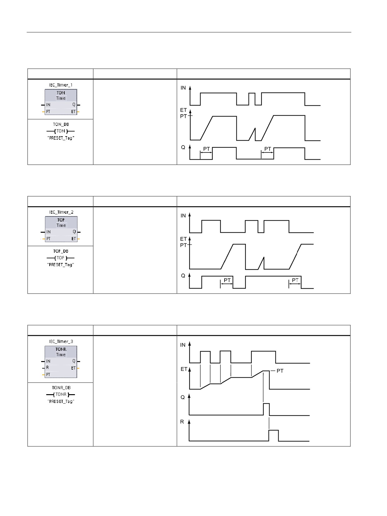
Programming made easy
6.3 Powerful instructions make programming easy
Table 6- 10 TON (ON-delay timer)
LAD / FBD
SCL
Timing diagram
"timer_db".TON(
IN:=_bool_in_,
PT:=_time_in_,
Q=>_bool_out_,
ET=>_time_out_);
Table 6- 11 TOF (OFF-delay timer)
LAD / FBD
SCL
Timing diagram
"timer_db".TOF(
IN:=_bool_in_,
PT:=_time_in_,
Q=>_bool_out_,
ET=>_time_out_);
Table 6- 12 TONR (ON-delay Retentive timer)
LAD / FBD
SCL
Timing diagram
"timer_db".TONR(
IN:=_bool_in_,
R:=_bool_in_,
PT:=_time_in_,
Q=>_bool_out_,
ET=>_time_out_);
114
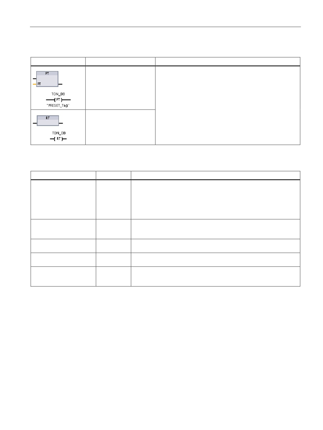
Programming made easy
6.3 Powerful instructions make programming easy
Table 6- 13 Preset timer -(PT)- and Reset timer -(RT)- coil instructions
LAD / FBD
SCL
Description
PRESET_TIMER(
Use the Preset timer -(PT)- and Reset timer -(RT)- coil instruc-
PT:=_time_in_,
tions with either box or coil timers. These coil instructions can be
placed in a mid-line position. The coil output power flow status is
TIMER:=_iec_timer_in_)
always the same as the coil input status.
;
• When the -(PT)- coil is activated, the PRESET time element
of the specified IEC_Timer DB data is set to the
"PRESET_Tag" time duration.
RESET_TIMER(
• When the -(RT)- coil is activated, the ELAPSED time element
_iec_timer_in_);
of the specified IEC_Timer DB data is reset to 0.
Table 6- 14 Data types for the parameters
Parameter
Data type
Description
Box: IN
Bool
TP, TON, and TONR:
Coil: Power flow
Box: 0=Disable timer, 1=Enable timer
Coil: No power flow=Disable timer, Power flow=Enable timer
TOF:
Box: 0=Enable timer, 1=Disable timer
Coil: No power flow=Enable timer, Power flow=Disable timer
R
Bool
TONR box only:
0=No reset
1= Reset elapsed time and Q bit to 0
Box: PT
Time
Timer box or coil: Preset time input
Coil: "PRESET_Tag"
Box: Q
Bool
Timer box: Q box output or Q bit in the timer DB data
Coil: DBdata.Q
Timer coil: you can only address the Q bit in the timer DB data
Box: ET
Time
Timer box: ET (elapsed time) box output or ET time value in the timer DB
Coil: DBdata.ET
data
Timer coil: you can only address the ET time value in the timer DB data.
115
Programming made easy
6.3 Powerful instructions make programming easy
Table 6- 15
Effect of value changes in the PT and IN parameters
Timer
Changes in the PT and IN box parameters and the corresponding coil parameters
TP
• Changing PT has no effect while the timer runs.
• Changing IN has no effect while the timer runs.
TON
• Changing PT has no effect while the timer runs.
• Changing IN to FALSE, while the timer runs, resets and stops the timer.
TOF
• Changing PT has no effect while the timer runs.
• Changing IN to TRUE, while the timer runs, resets and stops the timer.
TONR
• Changing PT has no effect while the timer runs, but has an effect when the timer resumes.
• Changing IN to FALSE, while the timer runs, stops the timer but does not reset the timer. Changing IN
back to TRUE will cause the timer to start timing from the accumulated time value.
PT (preset time) and ET (elapsed time) values are stored in the specified IEC_TIMER DB
data as signed double integers that represent milliseconds of time. TIME data uses the T#
identifier and can be entered as a simple time unit (T#200ms or 200) and as compound time
units like T#2s_200ms.
Table 6- 16
Size and range of the TIME data type
Data type
Size
Valid number ranges1
TIME
32 bits, stored as
T#-24d_20h_31m_23s_648ms to T#24d_20h_31m_23s_647ms
DInt data
Stored as -2,147,483,648 ms to +2,147,483,647 ms
1
The negative range of the TIME data type shown above cannot be used with the timer instructions. Negative PT (preset
time) values are set to zero when the timer instruction is executed. ET (elapsed time) is always a positive value.
116

Programming made easy
6.3 Powerful instructions make programming easy
Timer programming
The following consequences of timer operation should be considered when planning and
creating your user program:
● You can have multiple updates of a timer in the same scan. The timer is updated each
time the timer instruction (TP, TON, TOF, TONR) is executed and each time the
ELAPSED or Q member of the timer structure is used as a parameter of another
executed instruction. This is an advantage if you want the latest time data (essentially an
immediate read of the timer). However, if you desire to have consistent values throughout
a program scan, then place your timer instruction prior to all other instructions that need
these values, and use tags from the Q and ET outputs of the timer instruction instead of
the ELAPSED and Q members of the timer DB structure.
● You can have scans during which no update of a timer occurs. It is possible to start your
timer in a function, and then cease to call that function again for one or more scans. If no
other instructions are executed which reference the ELAPSED or Q members of the timer
structure, then the timer will not be updated. A new update will not occur until either the
timer instruction is executed again or some other instruction is executed using ELAPSED
or Q from the timer structure as a parameter.
● Although not typical, you can assign the same DB timer structure to multiple timer
instructions. In general, to avoid unexpected interaction, you should only use one timer
instruction (TP, TON, TOF, TONR) per DB timer structure.
Self-resetting timers are useful to trigger actions that need to occur periodically. Typically,
self-resetting timers are created by placing a normally-closed contact which references the
timer bit in front of the timer instruction. This timer network is typically located above one or
more dependent networks that use the timer bit to trigger actions. When the timer expires
(elapsed time reaches preset value), the timer bit is ON for one scan, allowing the dependent
network logic controlled by the timer bit to execute. Upon the next execution of the timer
network, the normally closed contact is OFF, thus resetting the timer and clearing the timer
bit. The next scan, the normally closed contact is ON, thus restarting the timer. When
creating self-resetting timers such as this, do not use the "Q" member of the timer DB
structure as the parameter for the normally-closed contact in front of the timer instruction.
Instead, use the tag connected to the "Q" output of the timer instruction for this purpose. The
reason to avoid accessing the Q member of the timer DB structure is because this causes an
update to the timer and if the timer is updated due to the normally closed contact, then the
contact will reset the timer instruction immediately. The Q output of the timer instruction will
not be ON for the one scan and the dependent networks will not execute.
The -(TP)-, -(TON)-, -(TOF)-, and -(TONR)- timer coils must be the last instruction in a
network. As shown in the timer example, a contact instruction in a subsequent network
evaluates the Q bit in a timer coil's IEC_Timer DB data. Likewise, you must address the
ELAPSED element in the IEC_timer DB data if you want to use the elapsed time value in
your program.
The pulse timer is started on a 0 to 1 transition of the Tag_Input bit value. The timer runs for
the time specified by Tag_Time time value.
117

Programming made easy
6.3 Powerful instructions make programming easy
As long as the timer runs, the state of DB1.MyIEC_Timer.Q=1 and the Tag_Output value=1.
When the Tag_Time value has elapsed, then DB1.MyIEC_Timer.Q=0 and the Tag_Output
value=0.
6.3.6
Counter operations
You use the counter instructions to count internal program events and external process
events.
● The "count up" counter (CTU) counts up by 1 when the value of the input parameter CU
changes from 0 to 1.
● The "count down" counter (CTD) counts down by 1 when the value of input parameter CD
changes from 0 to 1.
● The "count up and down" counter (CTUD) counts up or down by 1 on the 0 to 1 transition
of the count up (CU) or count down (CD) inputs.
S7-1200 also provides high-speed counters (Page 129) (HSC) for counting events that occur
faster than the OB execution rate.
The CU, CD, and CTUD instructions use software counters whose maximum counting rate is
limited by the execution rate of the OB they are placed in.
Note
If the events to be counted occur within the execution rate of the OB, use CTU, CTD, or
CTUD counter instructions. If the events occur faster than the OB execution rate, then use
the HSC.
Each counter uses a structure stored in a data block to maintain counter data. For SCL, you
must first create the DB for the individual counter instruction before you can reference it. For
LAD and FBD, STEP 7 automatically creates the DB when you insert the instruction.
118
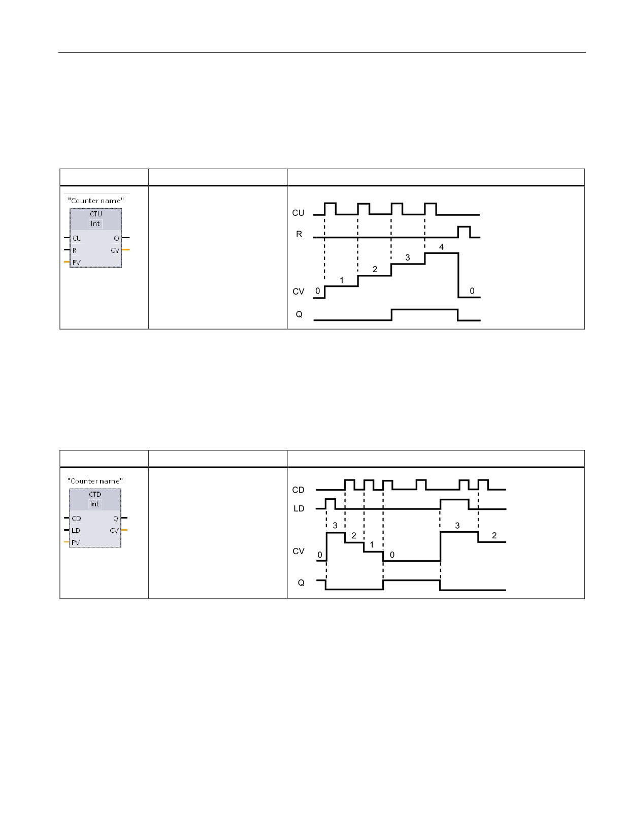
Programming made easy
6.3 Powerful instructions make programming easy
The number of counters that you can use in your user program is limited only by the amount
of memory in the CPU. Individual counters use 3 bytes (for SInt or USInt), 6 bytes (for Int or
UInt), or 12 bytes (for DInt or UDInt).
Table 6- 17 CTU (count up) counter
LAD / FBD
SCL
Operation
"ctu_db".CTU(
CU:=_bool_in,
R:=_bool_in,
PV:=_in_,
Q=>_bool_out,
CV=>_out_);
The timing diagram shows the operation of a CTU counter with an unsigned integer count
value (where PV = 3).
● If the value of parameter CV (current count value) is greater than or equal to the value of
parameter PV (preset count value), then the counter output parameter Q = 1.
● If the value of the reset parameter R changes from 0 to 1, then CV is reset to 0.
Table 6- 18 CTD (count down) counter
LAD / FBD
SCL
Operation
"ctd_db".CTD(
CD:=_bool_in,
LD:=_bool_in,
PV:=_in_,
Q=>_bool_out,
CV=>_out_);
The timing diagram shows the operation of a CTD counter with an unsigned integer count
value (where PV = 3).
● If the value of parameter CV (current count value) is equal to or less than 0, the counter
output parameter Q = 1.
● If the value of parameter LD changes from 0 to 1, the value at parameter PV (preset
value) is loaded to the counter as the new CV.
119
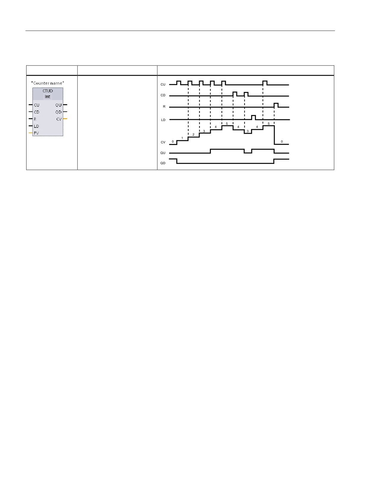
Programming made easy
6.3 Powerful instructions make programming easy
Table 6- 19 CTUD (count up and down) counter
LAD / FBD
SCL
Operation
"ctud_db".CTUD(
CU:=_bool_in,
CD:=_bool_in,
R:=_bool_in,
LD:=_bool_in,
PV:=_in_,
QU=>_bool_out,
QD=>_bool_out,
CV=>_out_);
The timing diagram shows the operation of a CTUD counter with an unsigned integer count
value (where PV = 4).
● If the value of parameter CV (current count value) is equal to or greater than the value of
parameter PV (preset value), then the counter output parameter QU = 1.
● If the value of parameter CV is less than or equal to zero, then the counter output
parameter QD = 1.
● If the value of parameter LD changes from 0 to 1, then the value at parameter PV is
loaded to the counter as the new CV.
● If the value of the reset parameter R changes from 0 to 1, CV is reset to 0.
120
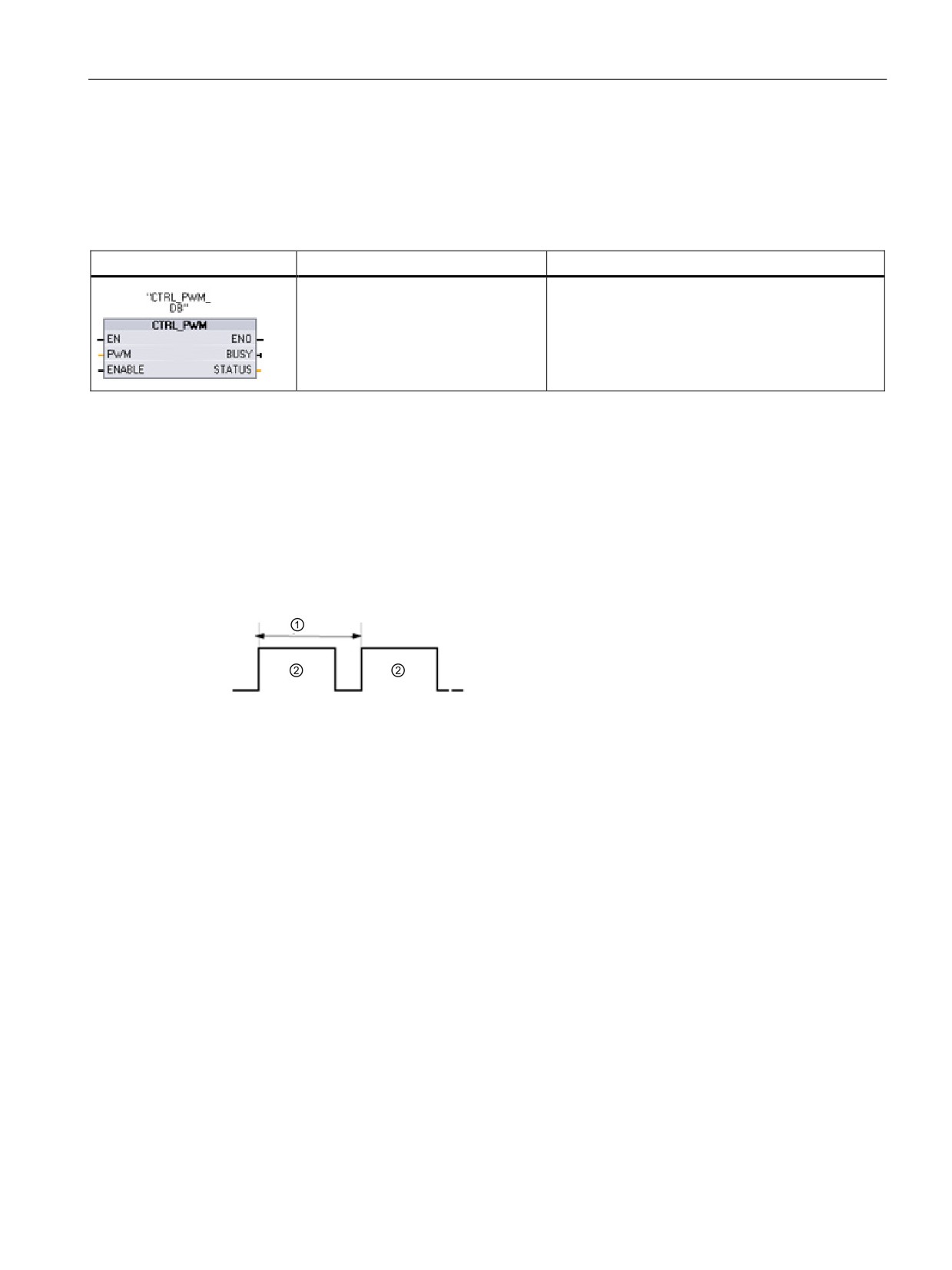
Programming made easy
6.3 Powerful instructions make programming easy
6.3.7
Pulse-width modulation (PWM)
The CTRL_PWM instruction is available in the Pulse group of the Extended instructions.
Table 6- 20
CTRL_PWM instruction
LAD / FBD
SCL
Desciption
"ctrl_pwm_db"(
The CTRL_PWM instruction provides a fixed cycle
PWM:=W#16#0,
time output with a variable duty cycle. The PWM
ENABLE:=False,
output runs continuously after being started at the
BUSY=>_bool_out_,
specified frequency (cycle time). The pulse width is
varied as required to affect the desired control.
STATUS=>_word_out_);
When you insert the CTRL_PWM instruction in your code block, you create the DB for the
instruction from the "Call options" dialog. The CTRL_PWM instruction stores the parameter
information in the DB and controls the data block parameters.
The pulse width will be set to the initial value configured in device configuration when the
CPU first enters the RUN mode. You write values to the word-length output (Q) address that
was specified in device configuration ("Output addresses" / "Start address") as needed to
change the pulse width. Use an instruction (such as Move, Convert, Math, or PID) to write
the specified pulse width to the appropriate word-length output (Q). You must use the valid
range for the output value (percent, thousandths, ten-thousandths, or S7 analog format).
Duty cycle can be expressed, for example, as a per-
centage of the cycle time or as a relative quantity (such
as 0 to 1000 or 0 to 10000). The pulse width can vary
from 0 (no pulse, always off) to full scale (no pulse,
always on).
① Cycle time
② Pulse width time
The PWM output can be varied from 0 to full scale, providing a digital output that in many
ways is the same as an analog output. For example, the PWM output can be used to control
the speed of a motor from stop to full speed, or it can be used to control position of a valve
from closed to fully opened.
121
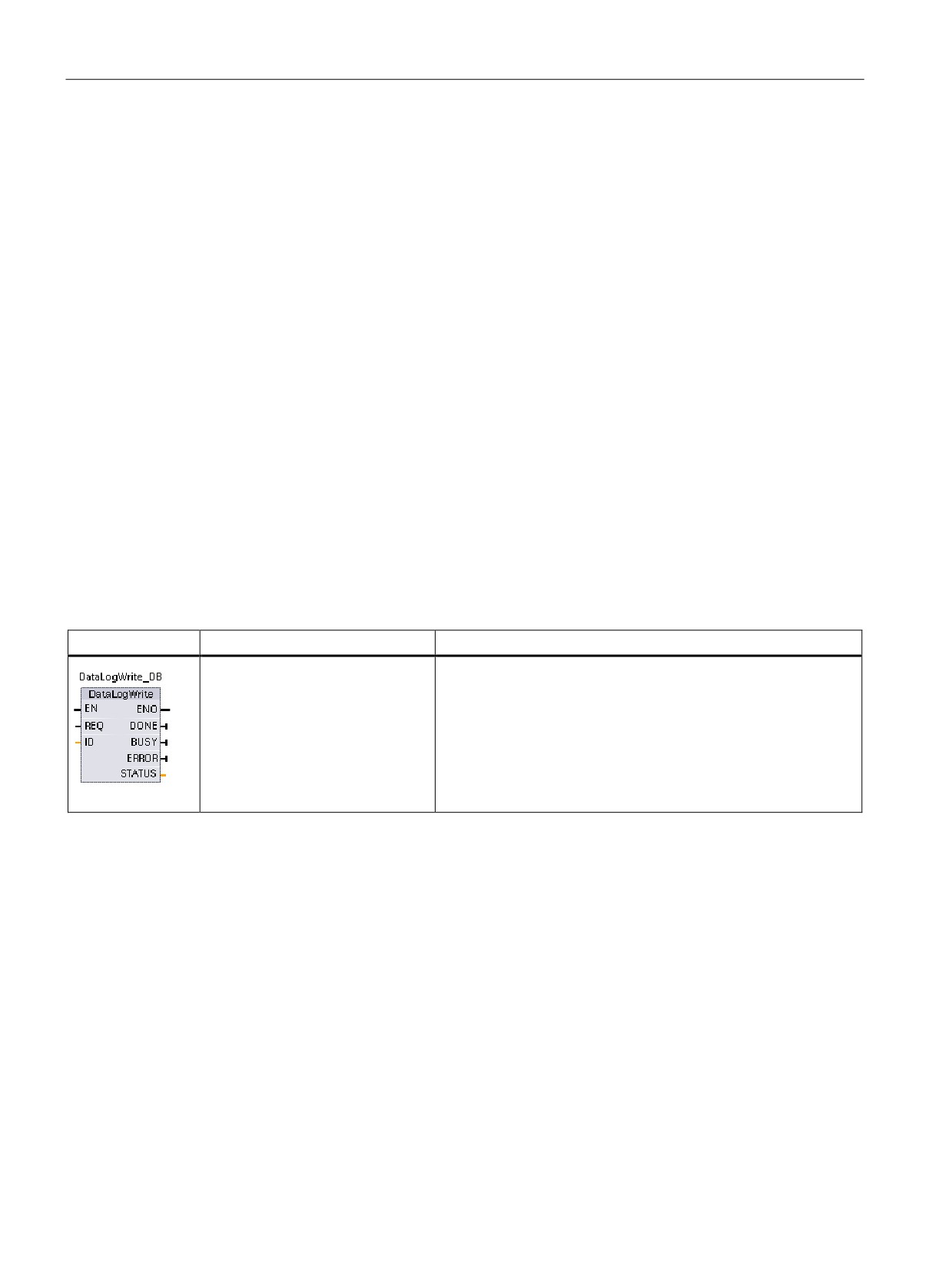
Programming made easy
6.4 Easy to create data logs
6.4
Easy to create data logs
Your control program can use the Data log instructions to store run-time data values in
persistent log files. The data log files are stored in flash memory (CPU or memory card). Log
file data is stored in standard CSV (Comma Separated Value) format. The data records are
organized as a circular log file of a pre-determined size.
The Data log instructions are used in your program to create, open, write a record, and close
the log files. You decide which program values will be logged by creating a data buffer that
defines a single log record. Your data buffer is used as temporary storage for a new log
record. New current values must be programmatically moved into the buffer during run-time.
When all of the current data values are updated, you can execute the DataLogWrite
instruction to transfer data from the buffer to a data log record.
You can open, edit, save, rename, and delete data log files from the File Browser page of
the Web Server. You must have read privileges to view the file browser and you must have
modify privileges to edit, delete, or rename data log files.
Use the DataLog instructions to programmatically store run-time process data in flash
memory of the CPU. The data records are organized as a circular log file of a pre-
determined size. New records are appended to the data log file. After the data log file has
stored the maximum number of records, the next record written overwrites the oldest record.
To prevent overwriting any data records, use the DataLogNewFile instruction. New data
records are stored in the new data log file, while the old data log file remains in the CPU.
Table 6- 21
DataLogWrite instruction
LAD/FBD
SCL
Description
"DataLogWrite_DB"(
DataLogWrite writes a data record into the specified data log.
req:=FALSE,
The pre-existing target data log must be open.
done=>_bool_out_,
You must programmatically load the record buffer with current
busy=>_bool_out_,
run-time data values and then execute the DataLogWrite instruc-
error=>_bool_out_,
tion to move new record data from the buffer to the data log.
status=>_word_out_,
If there is a power failure during an incomplete DataLogWrite
ID:=_dword_inout_);
operation, then the data record being transferred to the data log
could be lost.
122