Siemens simatic S7-200. Product Information
Product Information
SIMATIC S7-200
X
2
EM231, EM232, EM235 Analog Input and Output Modules
Release
3
4
This Product Information exists in electronic form only. You can print a paper copy by
selecting File " Print from the menu.
New Expansion Modules Available
The following expansion modules have been added to the S7-200 family. The order
numbers for these expansion modules are shown below:
S EM231 Analog Input AI 4 x 12 Bits
(order number 6ES7 231-0HC20-0XA0)
S EM232 Analog Output AQ 2 x 12 Bits
(order number 6ES7-232-0HB20-0XA0)
S EM235 Analog Combo AI 4/AQ 1 x 12 Bits
(order number 6ES7 235-0KD20-0XA0)
The technical specifications for the expansion modules are included in this product
information document. You can refer to the S7-200 Programmable Controller System
Manual for more information about the S7-200 product family.
Additional Assistance
For assistance in answering technical questions, for training on this product, or for
ordering, contact your Siemens distributor or sales office.
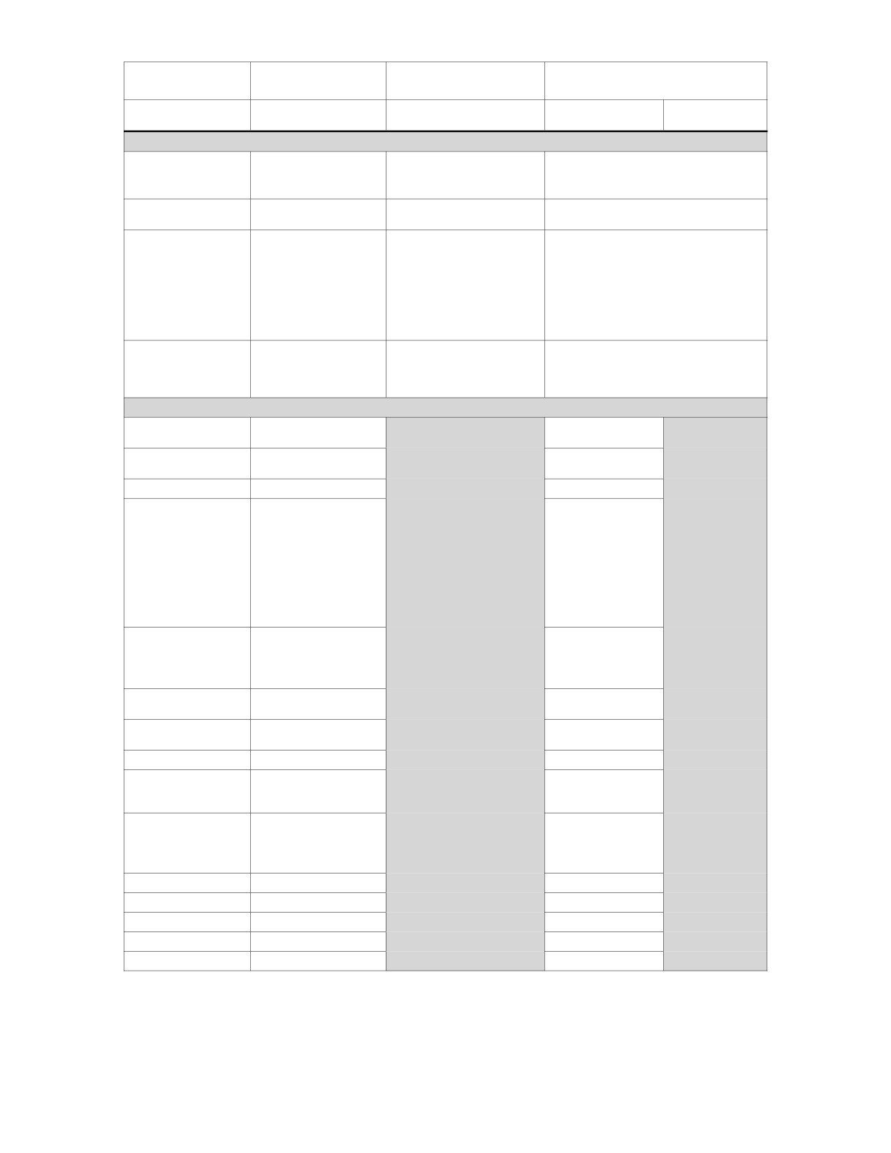
Description
EM231 Analog Input
EM232 Analog Output
EM235 Analog Combo
Order Number
AI 4 x 12 Bits
AQ 2 x 12 Bits
AI 4/AQ 1 x 12 Bits
6ES7 231-0HC20-0XA0
6ES7 232-0HB20-0XA0
6ES7 235-0KD20-0XA0
Input Specifications
Output Specifications
Input Specifications
Output
Specifications
General Specifications
Dimensions (W x H x D)
71.2 mm x 80 mm x 62 mm
46 mm x 80 mm x 62 mm
71.2 mm x 80 mm x 62 mm
Weight
183 g
148 g
186 g
Power loss (dissipation)
2 W
2 W
2 W
Number of physical I/O
4 analog input points
2 analog output points
4 analog input points,
1 analog output point
Power Consumption
From +5 VDC (from I/O
20 mA
20 mA
30 mA
bus)
From L+
60 mA
70 mA (with both outputs at 20
60 mA (with output at 20 mA)
mA)
L+ voltage range,
20.4 to 28.8
20.4 to 28.8
20.4 to 28.8
Class 2 or DC sensor
supply
LED indicator
24 VDC Power Supply
24 VDC Power Supply Good,
24 VDC Power Supply Good,
Good,
ON = no fault,
ON = no fault,
ON = no fault,
OFF = no 24 VDC power
OFF = no 24 VDC power
OFF = no 24 VDC power
Analog Input Specifications
No. of Analog Input
4
4
Points
Isolation (Field side to
None
None
logic circuit)
Input type
Differential
Differential
Input ranges
Voltage (unipolar)
0 to 10 V, 0 to 5 V
0 to 10 V, 0 to 5 V,
0 to 1 V, 0 to 500 mV,
0 to 100 mV, 0 to 50 mV
Voltage (bipolar)
±5 V, ± 2.5 V
± 10 V, ± 5 V, ± 2.5 V,
± 1 V, ± 500 mV,
± 250 mV, ± 100 mV,
± 50 mV, ± 25 mV
Current
0 to 20 mA
0 to 20 mA
Input Resolution
see Table 1
see Table 2
Voltage (unipolar)
Voltage (bipolar)
Current
Analog to digital
< 250 µs
< 250 µs
conversion time
Analog input step
1.5 ms to 95%
1.5 ms to 95%
response
Common mode rejection
40 dB, DC to 60 Hz
40 dB, DC to 60 Hz
Common mode voltage
Signal voltage plus
Signal voltage plus
common mode voltage
common mode voltage
(must be ≤ 12 V)
(must be ≤ 12 V)
Data word format
(see Figure 3)
(see Figure 3)
Bipolar, full-scale range
-32000 to +32000
-32000 to +32000
Unipolar, full-scale
0 to 32000
0 to 32000
range
Input impedance
≥10 MΩ
≥ 10 MΩ
Input filter attenuation
-3 db @ 3.1 Khz
-3 db @ 3.1 Khz
Maximum input voltage
30 VDC
30 VDC
Maximum input current
32 mA
32 mA
Resolution
12 bit A/D converter
12 bit A/D converter

Description
EM231 Analog Input
EM232 Analog Output
EM235 Analog Combo
Order Number
AI4x12 Bits
AQ2x12 Bits
AI4/AQ 1 x 12 Bits
6ES7 231-0HC20-0XA0
6ES7 232-OHB20-0XA0
6ES7 235-0KD20-0XA0
Input Specifications
Output Specifications
Input Specifications
Output
Specifications
Analog Output Specifications
No. of Analog Output
2
1
Points
Isolation (Field side to
None
None
logic circuit)
Signal range
Voltage output
± 10 V
± 10 V
Current output
0 to 20 mA
0 to 20 mA
Resolution, full-scale
Voltage
12 bits
12 bits
Current
11 bits
11 bits
Data word format
Voltage
-32000 to +32000
-32000 to +32000
Current
0 to +32000
0 to +32000
Accuracy
Worst case, 0° to 55° C
Voltage output
± 2% of full-scale
± 2% of full-scale
Current output
± 2% of full-scale
± 2% of full-scale
Typical, 25° C
Voltage output
± 0.5% of full-scale
± 0.5% of full-scale
Current output
± 0.5% of full-scale
± 0.5% of full-scale
Settling time
Voltage output
100 µS
100 µS
Current output
2 mS
2 mS
Maximum drive
Voltage output
5000 Ω minimum
5000 Ω minimum
Current output
500 Ω maximum
500 Ω maximum
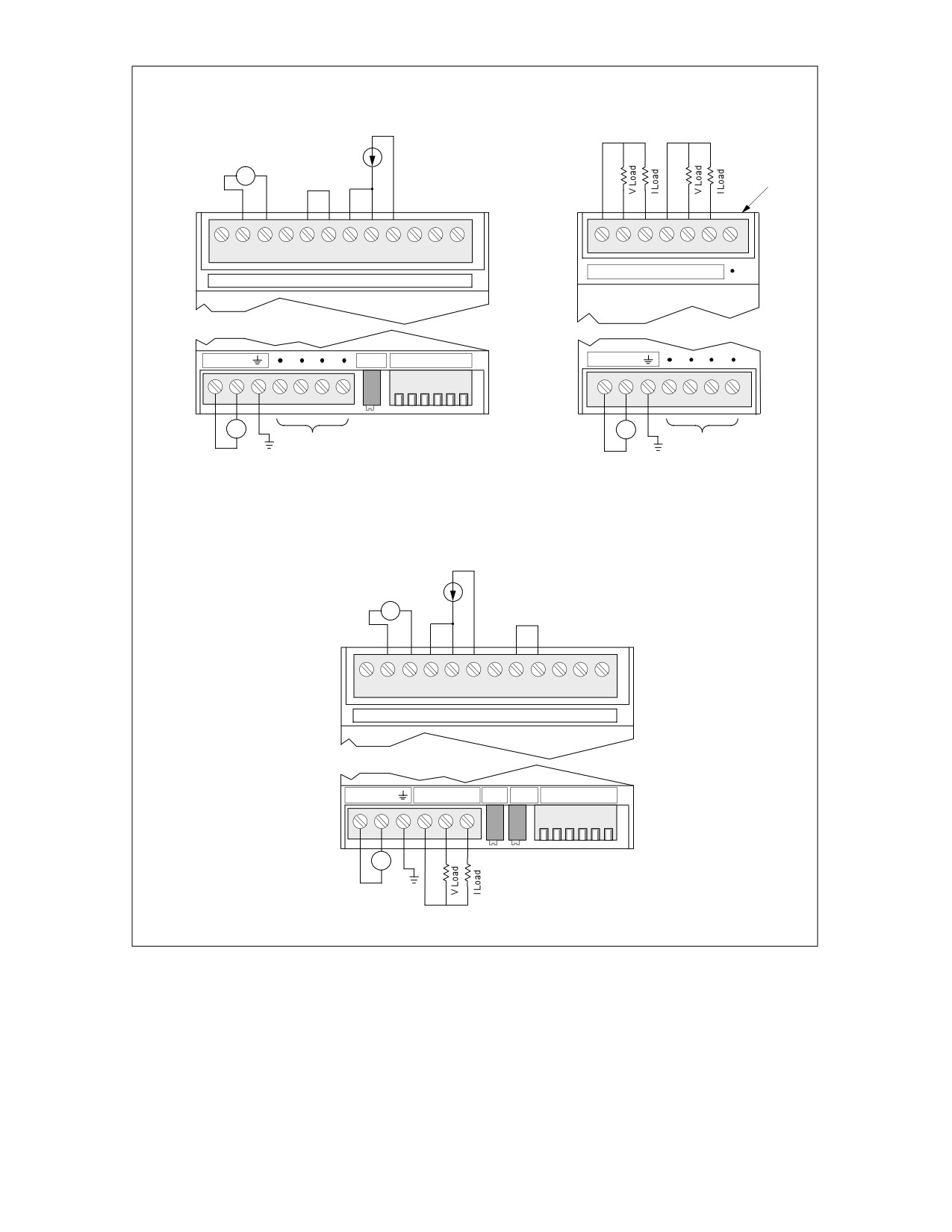
EM231
EM232
Current transmitter
Voltage transmitter
+ -
Unused input
Not used
M0
V0
I0
M1
V1
I1
RA A+ A - RB B+ B - RC C+ C-
RD D+
D-
EM232
EM231
AQ 2 x 12 Bit
AI 4
M L+
Gain
Configuration
M L+
+
+
24V
24V
-
Not used
-
Not used
24 VDC power and
24 VDC power and
common terminals
common terminals
EM235
Current transmitter
Voltage transmitter
+ -
Unused input
RA A+ A - RB B+ B - RC C+ C-
RD D+
D-
EM235
AI 4/AQ 1
M L+
M0
V0
I0
Gain
Offset
Configuration
+
24V
-
24 VDC power and
common terminals
Figure 1
Connector Terminal Identification for Expansion Modules EM231, EM232, and EM235
Input Calibration
The calibration adjustments affect the instrumentation amplifier stage that follows the
analog multiplexer (see Figure 4). Therefore, calibration affects all user input channels.
Variations in the component values of each input circuit preceeding the analog
multiplexer will cause slight differences in the readings between channels connected to
the same input signal even after calibration.
To meet the specifications contained in this data sheet, you should enable analog input
filters for all inputs of the module. Select 64 or more samples in calculating the
average value. For more information about analog input filters, see the S7-200
Programmable Controller System Manual.
To calibrate the input, use the following steps.
1. Turn off the power to the module. Select the desired input range.
2. Turn on the power to the CPU and module. Allow the module to stabilize for 15
minutes.
3. Using a transmitter, a voltage source, or a current source, apply a zero value signal
to one of the input terminals.
4. Read the value reported to the CPU by the appropriate input channel.
5. Adjust the OFFSET potentiometer until the reading is zero, or the desired digital
data value.
6. Connect a full-scale value signal to one of the input terminals. Read the value
reported to the CPU.
7. Adjust the GAIN potentiometer until the reading is 32000, or the desired digital data
value.
8. Repeat OFFSET and GAIN calibration as required.
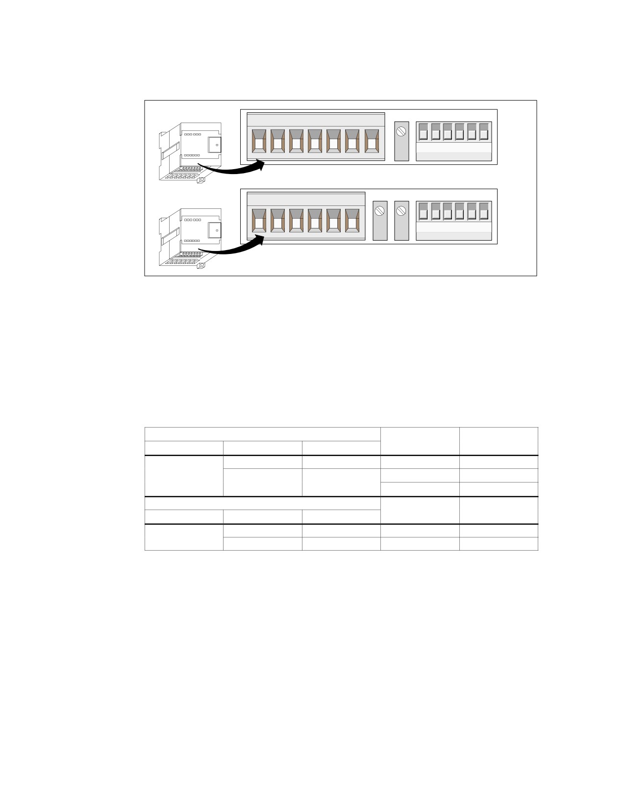
Calibration and Configuration Location for EM231 and EM235
The calibration potentiometer and configuration DIP switches are located on the right
of the bottom terminal block of the module, as shown in Figure 2.
EM231
↑ On
↓ Off
1
2
3
4
5
6
DIP
ON ↑
Fixed Terminal Block
Gain
Configuration
EM235
↑ On
↓ Off
1
2
3
4
5
6
DIP
ON ↑
Fixed Terminal Block
Gain Offset
Configuration
Figure 2
Calibration Potentiometer and Configuration DIP Switches for EM231 and EM235
Configuration for EM231
Table 1 shows how to configure the EM231 module using the configuration DIP
switches. Switches 1, 2, and 3 select the analog input range. All inputs are set to the
same analog input range. In this table, ON is closed, and OFF is open.
Table 1
EM231 Configuration Switch Table to Select Analog Input Range
Unipolar
Full-Scale Input
Resolution
SW1
SW2
SW3
OFF
ON
0 to 10 V
2.5 mV
ON
0 to 5 V
1.25 mV
ON
OFF
0 to 20 mA
5 µA
Bipolar
Full-Scale Input
Resolution
SW1
SW2
SW3
OFF
ON
± 5 V
2.5 mV
OFF
ON
OFF
± 2.5 V
1.25 mV
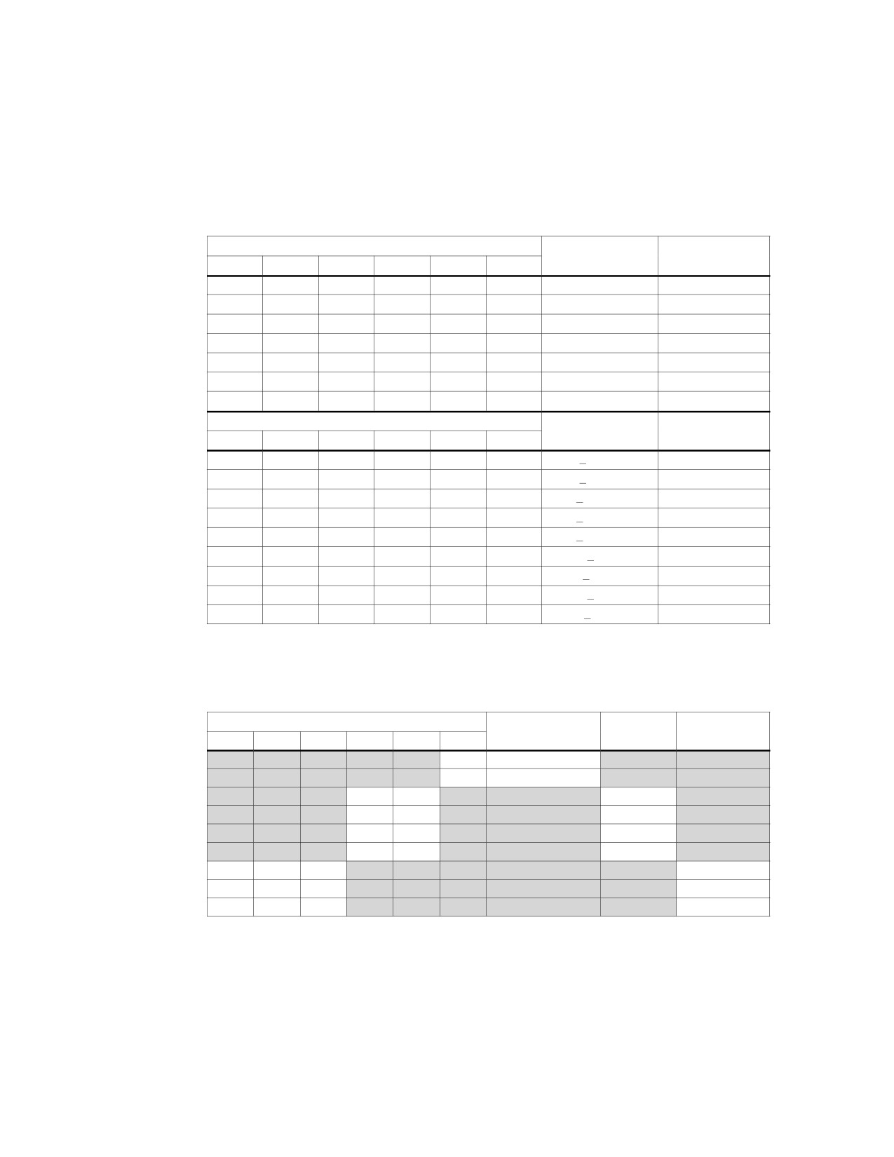
Configuration for EM235
Table 2 shows how to configure the EM235 module using the configuration DIP
switches. Switches 1 through 6 select the analog input range and resolution. All inputs
are set to the same analog input range and format. Table 3 shows how to select for
unipolar/bipolar (switch 6), gain (switches 4 and 5), and attenuation (switches 1, 2, and
3). In these tables, ON is closed, and OFF is open.
Table 2
EM235 Configuration Switch Table to Select Analog Input Range and Resolution
Unipolar
Full-Scale Input
Resolution
SW1
SW2
SW3
SW4
SW5
SW6
ON
OFF
OFF
ON
OFF
ON
0 to 50 mV
12.5 mV
OFF
ON
OFF
ON
OFF
ON
0 to 100 mV
25 mV
ON
OFF
OFF
OFF
ON
ON
0 to 500 mV
125 mV
OFF
ON
OFF
OFF
ON
ON
0 to 1 V
250 mV
ON
OFF
OFF
OFF
OFF
ON
0 to 5 V
1.25 mV
ON
OFF
OFF
OFF
OFF
ON
0 to 20 mA
5 mA
OFF
ON
OFF
OFF
OFF
ON
0 to 10 V
2.5 mV
Bipolar
Full-Scale Input
Resolution
SW1
SW2
SW3
SW4
SW5
SW6
ON
OFF
OFF
ON
OFF
OFF
+25 mV
12.5 mV
OFF
ON
OFF
ON
OFF
OFF
+50 mV
25 mV
OFF
OFF
ON
ON
OFF
OFF
+100 mV
50 mV
ON
OFF
OFF
OFF
ON
OFF
+250 mV
125 mV
OFF
ON
OFF
OFF
ON
OFF
+500 mV
250 mV
OFF
OFF
ON
OFF
ON
OFF
+1 V
500 mV
ON
OFF
OFF
OFF
OFF
OFF
+2.5 V
1.25 mV
OFF
ON
OFF
OFF
OFF
OFF
+5 V
2.5 mV
OFF
OFF
ON
OFF
OFF
OFF
+10 V
5 mV
Table 3
EM235 Configuration Switch Table to Select Unipolar/Bipolar, Gain, and
Attenuation
EM235 Configuration Switches
Unipolar/Bipolar
Attenuation
Gain Select
SW1
SW2
SW3
SW4
SW5
SW6
Select
Select
ON
Unipolar
OFF
Bipolar
OFF
OFF
x1
OFF
ON
x10
ON
OFF
x100
ON
ON
invalid
ON
OFF
OFF
0.8
OFF
ON
OFF
0.4
OFF
OFF
ON
0.2

Input Data Word Format for EM231 and EM235
Figure 3 shows where the 12-bit data value is placed within the analog input word of
the CPU.
MSB
LSB
15
14
3
2
0
AIW XX
0
Data value12 Bits
0
0
0
Unipolar data
MSB
LSB
15
4
3
0
AIW XX
Data
value
12 Bits
0
0
0
0
Bipolar data
Figure 3
Input Data Word Format for EM231 and EM235
Note
The 12 bits of the analog-to-digital converter (ADC) readings are left-justified in the
data word format. The MSB is the sign bit: zero indicates a positive data word value.
In the unipolar format, the three trailing zeros cause the data word to change by a
count of eight for each one-count change in the ADC value. In the bipolar format, the
four trailing zeros cause the data word to change by a count of sixteen for each one
count change in the ADC value.
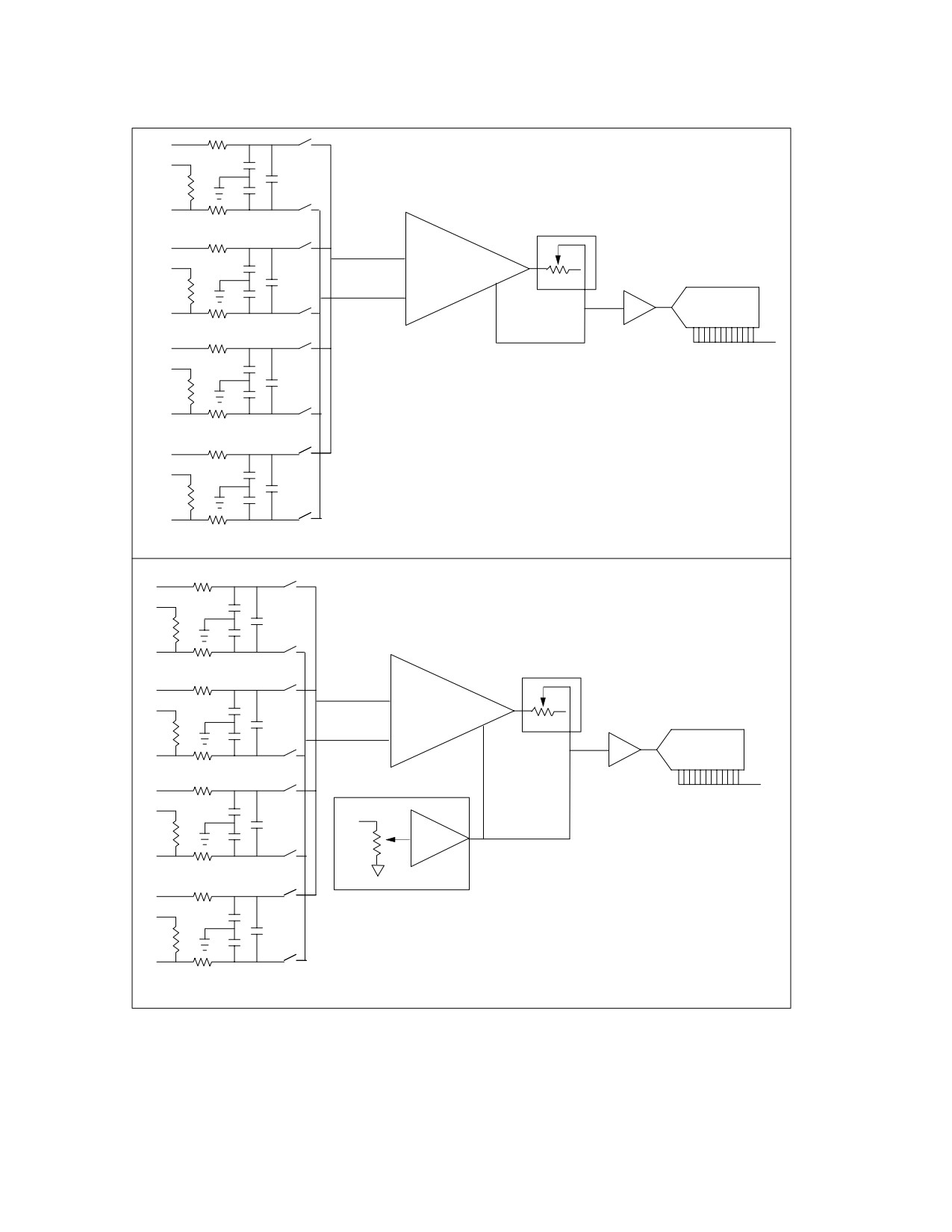
Input Block Diagram for EM231 and EM235
Figure 4 shows the EM231 and EM235 input block diagrams.
A+
R
EM231
RA
C
C
Rloop
C
A-
GAIN ADJUST
A=1
R
+
B+
R
Instrumentation
RB
C
AMP
C
BUFFER
Rloop
C
-
A/D Converter
B-
R
A=2
11
0
C+
R
RC
C
C
Rloop
C
C-
A=3
R
D+
R
RD
C
C
Rloop
C
D-
A=4
R
Input filter
MUX 4 to 1
EM235
A+
R
RA
C
C
Rloop
C
A-
GAIN ADJUST
A=1
R
+
B+
Analog-to-digital converter
R
Instrumentation
RB
C
AMP
C
BUFFER
Rloop
C
-
A/D Converter
B-
A=2
R
DATA
11
0
C+
R
RC
C
REF_VOLT
C
+
Rloop
C
Buffer
C-
-
A=3
R
Offset Adjust
D+
R
RD
C
C
Rloop
C
D-
A=4
R
Input filter
MUX 4 to 1
Figure 4
EM231 and EM235 Input Block Diagram
Output Data Word Format for EM232 and EM235
Figure 5 shows where the 12-bit data value is placed within the analog output word of
the CPU.
MSB
LSB
15
14
4
3
0
AQW XX
0
Data value
11 Bits
0
0
0
0
Current output data format
MSB
LSB
15
4
3
0
AQW XX
Data
value
12 Bits
0
0
0
0
Voltage output data format
Figure 5
Output Data Word Format for EM232 and EM235
Note
The 12 bits of the digital-to-analog converter (DAC) readings are left-justified in the
output data word format. The MSB is the sign bit: zero indicates a positive data word
value. The four trailing zeros are truncated before being loaded into the DAC
registers. These bits have no effect on the output signal value.
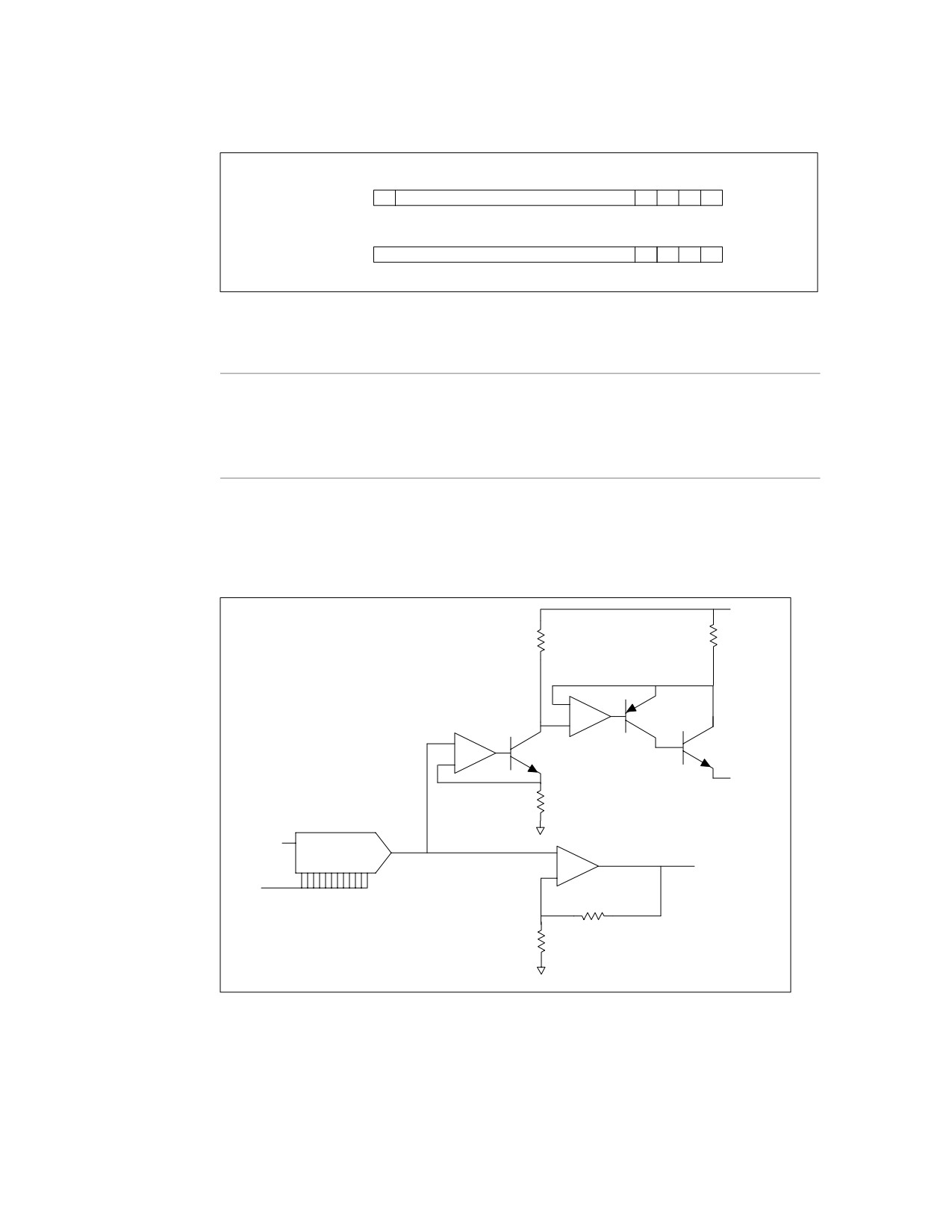
Output Block Diagram for EM232 and EM235
Figure 6 shows the EM232 and EM235 output block diagrams.
+24 Volt
R
100
-
+
+
-
Voltage-to-current converter
Iout
R
0..20 mA
M
Vref
D/A converter
+
+/- 2V
Vout
-
11
0
-10.. +10 Volts
DATA
R
Digital-to-analog converter
1/4
R
Voltage output buffer
M
Figure 6
EM232 and EM235 Output Block Diagram
Installation Guidelines
Use the following guidelines to ensure good accuracy and repeatability:
S Ensure that the 24-VDC Sensor Supply is free of noise and is stable.
S Use the shortest possible sensor wires.
S Use shielded twisted pair wiring for sensor wires.
S Terminate the shield at the Sensor location only.
S Short the inputs for any unused channels, as shown in Figure 1.
S Avoid bending the wires into sharp angles.
S Use wireways for wire routing.
S Avoid placing signal wires parallel to high-energy wires. If the two wires must meet,
cross them at right angles.
S Ensure that the input signals are within the common mode voltage specification by
isolating the input signals or referencing them to the external 24V common of the
analog module.
Note
The EM231 and EM235 expansion modules are not recommended for use with
thermocouples.
Understanding and Using the Analog Input Module: Accuracy and Repeatability
The EM231 and EM235 analog input modules are low-cost, high-speed 12 bit analog
input modules. The modules are capable of converting an analog input to its
corresponding digital value in 149 µsec. Conversion of the analog signal input is
performed each time the analog point is accessed by your program. These times must
be added to the basic execution time of the instruction used to access the analog
input.
The EM231 and EM235 provide an unprocessed digital value (no linearization or
filtering) that corresponds to the analog voltage or current presented at the module’s
input terminals. Since the modules are high-speed modules, they can follow rapid
changes in the analog input signal (including internal and external noise).
Reading-to-reading variations caused by noise for a constant or slowly changing
analog input signal can be minimized by averaging a number of readings. As the
number of readings used in computing the average value increases, a correspondingly
slower response time to changes in the input signal can be observed.
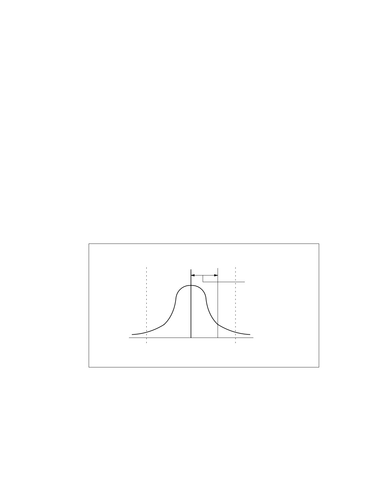
The specifications for repeatability describe the reading-to-reading variations of the
module for an input signal that is not changing. The repeatability specification defines
the limits within which 99% of the readings will fall. The mean accuracy specification
describes the average value of the error (the difference between the average value of
individual readings and the exact value of the actual analog input signal). The
repeatability is described in Figure 7 by the bell curve. This figure shows the 99%
repeatability limits, the mean or average value of the individual readings, and the mean
accuracy in a graphical form. Table 4 gives the repeatability specifications and the
mean accuracy as they relate to each of the configurable ranges.
Average
Signal
Value
Input
Mean (average)
Accuracy
Repeatability limits
(99% of all readings fall within these limits)
Figure 7
Accuracy Definitions

Table 4
EM231 and EM235 Specifications
Repeatability1
Mean (average) Accuracy1,2,3,4
Full Scale Input Range
% of Full Scale
Counts
% of Full Scale
Counts
EM231 Specifications
0 to 5 V
0 to 20 mA
± 24
± 0.01%
0 to 10 V
± 0.075%
± 32
± 2.5 V
±
48
±
0.05%
± 5 V
EM235 Specifications
0 to 50 mV
± 0.25%
± 80
0 to 100 mV
± 0.2%
± 64
0 to 500 mV
0 to 1 V
± 0.075%
± 24
0 to 5 V
± 0.05%
± 16
0 to 20 mA
0 to 10 V
± 25 mV
± 0.25%
± 160
± 50 mV
± 0.2%
± 128
± 100 mV
± 0.1%
± 64
± 250 mV
± 500 mV
± 0.075%
± 48
± 1 V
±
0.05%
±
32
± 2.5 V
± 5 V
± 10 V
1
Measurements made after the selected input range has been calibrated.
2
The offset error in the signal near zero analog input is not corrected, and is not included in the accuracy specifications.
3
There is a channel-to-channel carryover conversion error, due to the finite settling time of the analog multiplexer. The
maximum carryover error is 0.1% of the difference between channels.
4
Mean accuracy includes effects of non-linearity and drift from 0 to 55 degrees C.
Definitions of the Analog Specifications
S Accuracy: deviation from the expected value on a given point.
S Resolution: the effect of an LSB change reflected on the output.
Agency Standards
These modules adhere to the following agency standards: UL 508 Listed (Industrial
Control Equipment); CSA C22.2 Number 142 Certified (Process Control Equipment);
FM Class I, Division 2, Groups A, B, C, & D Hazardous Locations, T4A; VDE 0160:
Electronic equipment for use in electrical power installations; European Community
(CE) Low Voltage Directive 73/23/EEC, EN 61131-2: Programmable controllers -
Equipment requirements; European Community (CE) EMC Directive 89/336/EEC.
For more information about these standards, refer to the S7-200 Programmable
Controller System Manual.